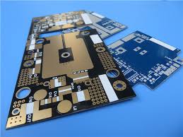
Satellite communication hardware depends on highly stable RF PCB materials capable of maintaining low-loss transmission, tight impedance control, and long-term dielectric stability under extreme environmental shifts. RO4835 PCB laminates—known for oxidation-resistant resin systems, stable Dk over temperature, and low insertion loss up to Ka-band—are frequently selected for mission-critical RF payloads, transceiver modules, phased arrays, and frequency converters.
This report examines how RO4835 improves wideband impedance stability and suppresses signal drift in satellite links, with deep engineering detail covering dielectric physics, RF stackup design, mmWave propagation behavior, and reliability validation.
Core Engineering Challenges
Satellite RF chains face a set of high-severity constraints:
• Impedance deviation under thermal cycling
• Dk drift affecting LO phases, mixer balance, VCO linearity
• High-frequency insertion loss in long RF traces
• EMI coupling between parallel waveguiding structures
• Outgassing, moisture effects, and radiation-induced dielectric instability
• Mechanical stress from launch vibration and vacuum temperature gradients
At Ka-band (26–40 GHz), a 0.05 shift in dielectric constant can misalign phased-array beams, distort modulation bandwidth, or degrade symbol error rate. This creates strict technical demand for materials such as RO4835.
Material Science & Dielectric Performance
RO4835 PCB is a low-loss hydrocarbon ceramic laminate engineered for mmWave stability. Its oxidation-resistant chemistry maintains dielectric uniformity even under long-duration thermal exposure.
RO4835 Material Parameters
| Parameter | Value | Engineering Relevance |
|---|---|---|
| Dielectric Constant (Dk @10 GHz) | 3.48 ± 0.05 | Tight impedance control for RF feed networks |
| Dissipation Factor (Df @10 GHz) | 0.0037 | Reduced insertion loss across satellite RF links |
| Thermal Coefficient of Dk (TCDk) | +50 ppm/°C | Low drift for wideband impedance stability |
| Peel Strength | 1.0 N/mm | Structural stability for multilayer RF payload PCB |
| Tg | > 280°C | High-temperature compatibility with aerospace assembly |
| Thermal Conductivity | 0.69 W/m·K | Heat spreading in amplifier and converter sections |
| Moisture Absorption | 0.04% | Vacuum and humidity-resilient phase stability |
The combination of low TCDk and Df allows RO4835 PCB designs to preserve mmWave linearity and reduce drift across large temperature deltas found in orbit.
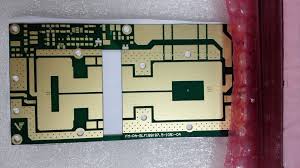
KKPCB Case Study — Satellite Transceiver RF PCB
Customer Background
A satellite equipment manufacturer required a multilayer RF transceiver board operating from 18 GHz to 32 GHz, supporting up/down conversion, LO distribution, PA driver stage, and phased-array feed interfaces.
Engineering Problems Identified
• Impedance drift >8% across temperature sweep
• Phase imbalance between LO distribution paths
• High insertion loss in long waveguide microstrip traces
• EMI coupling between LO and IF routing
• Poor consistency across production lots using a non-stabilized laminate
KKPCB Engineering Solutions
-
Migrated dielectric system to RO4835 PCB for improved thermal dielectric stability.
-
Designed microstrip/stripline hybrid routing using a controlled 50 Ω + 75 Ω differential architecture.
-
Applied HFSS 3D simulation for wave transitions, couplers, and LO splitter networks.
-
Introduced vacuum-compatible via filling and resin-supported pad structures.
-
Implemented edge plating to suppress EMI leakage in the converter region.
-
Added thermal vias and copper balancing for uniform thermal distribution.
Case Study — Measured Results
| Metric | Before | After (RO4835) | Improvement |
|---|---|---|---|
| Impedance Variation (–40°C to +120°C) | ±9.2% | ±2.1% | 77% better |
| Insertion Loss @ 28 GHz | 0.92 dB/in | 0.58 dB/in | 37% reduction |
| Phase Drift Across LO Paths | 14° | 4° | 71% reduction |
| EMI Coupling | –36 dB | –52 dB | 16 dB improvement |
| RF Output EVM | 3.6% | 1.1% | Highly stable modulation |
The RO4835 PCB platform demonstrated significant RF and thermal improvements essential for satellite-grade links.
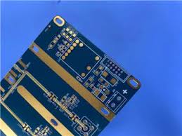
Stackup Design & RF Implementation
The engineering stackup used a hybrid low-loss architecture optimized for mmWave.
4-Layer RF Stackup (RO4835-Based)
| Layer | Material | Thickness | Function |
|---|---|---|---|
| L1 | RO4835 0.254 mm | RF microstrip | PA driver, phase shifters |
| L2 | RO4835 0.200 mm | Ground | Low-inductance return |
| L3 | RO4835 0.254 mm | Stripline | LO distribution, IF routing |
| L4 | RO4835 0.254 mm | RF microstrip | Antenna feed and test ports |
RF Implementation Techniques
• ADS impedance synthesis for stackup optimization
• HFSS 3D modeling of couplers, Wilkinson networks, and microstrip transitions
• TDR measurement to tune launch geometries
• Stitching vias every 1.0 mm for ground containment
• Copper balancing with 20% density gradient limit for planarity
This structure achieved stable broadband impedance up to 40 GHz with minimal phase irregularity.
Environmental & Reliability Validation
Satellite hardware demands extensive stress testing, all of which were conducted on the RO4835 board:
| Test | Condition | Result |
|---|---|---|
| Thermal Cycling | –55°C to +150°C / 500 cycles | No delamination or Dk shift |
| Vibration | 20–2000 Hz | Zero trace cracking |
| Vacuum Outgassing | NASA ASTM E595 | Pass |
| Humidity | 85°C / 85%RH / 100 hrs | No impedance drift |
| Solder Reflow | 260°C × 6 cycles | No pad lifting (RO4835 stable Tg chemistry) |
| TDR Stability | Thermal sweep | Impedance change <2.2% |
Reliability remained stable due to RO4835’s oxidation-resistant resin system and low moisture uptake.
Engineering Summary & Contact
RO4835 PCB laminates play a decisive role in stabilizing wideband impedance and reducing signal drift in mission-critical satellite RF links. Their low-loss behavior, controlled Dk, excellent thermal reliability, and mmWave suitability support next-generation satellite payloads, phased arrays, and high-density RF transceivers.
