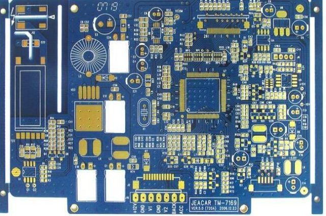
In the precision chain of modern electronics manufacturing, PCBA processing (Printed Circuit Board Assembly) serves as the critical stage that gives electronic products “life.” During this process, electronic components are precisely soldered onto a printed circuit board (PCB) to form a complete circuit system.
However, PCB board deformation is a hidden issue that can severely affect the performance, reliability, and appearance of electronic products once it occurs.
I. Causes of Deformation: The “Butterfly Effect” of Materials and Processes
A PCB is composed of multiple composite materials — such as copper foil, resin, and glass cloth. Due to the differences in their physical and chemical properties, residual thermal stress is inevitably generated during the lamination process. This stress becomes an inherent hidden danger that can lead to deformation.
Beyond material characteristics, various external factors can also amplify the deformation risk:
-
Temperature fluctuations during processing or storage
-
Uneven electroplating or inconsistent copper thickness
-
Improper board thickness and dimension design
-
Unbalanced soldering temperature profiles
-
Mechanical stress during handling or component placement
These interacting factors create a “butterfly effect” — small variations during production that can ultimately change the PCB’s overall shape and performance.
II. Hazard Chain: From Microscopic Defects to System Failures
Once PCB deformation occurs, the consequences ripple throughout the entire production and product lifecycle:
-
Soldering Failures:
Deformation alters solder joint spacing, leading to cold solder joints, bridging, or detachment. Circuit reliability drops sharply, increasing the failure rate. -
Assembly Misalignment:
Inaccurate positioning of components causes misconnections and affects product functionality.

-
Structural Fragility:
A warped board has lower mechanical strength and is more prone to cracking or breaking during assembly, shipping, or use. -
Signal Instability:
Deformation changes trace lengths and impedance, leading to signal attenuation, crosstalk, or timing errors—critical issues in high-speed circuits. -
Thermal Management Problems:
Misalignment of heat sinks or fans prevents proper cooling, leading to overheating and shortened component lifespan. -
Appearance and Quality Issues:
Visible board warping reduces aesthetic value and consumer trust, while also delaying production due to rework and debugging needs.
III. Prevention Strategies: Full-Process Quality Control
To eliminate PCB deformation risks, PCBA manufacturers should adopt a comprehensive prevention and control system across every stage of production.
1. Material Selection
-
Choose substrates with matched thermal expansion coefficients (CTE).
-
Prioritize materials offering high thermal and mechanical stability.
2. Process Optimization
-
Control temperature profiles during soldering and reflow to avoid localized overheating.
-
Distribute stress concentration areas by optimizing PCB layout and stack-up.
-
Continuously improve lamination, electroplating, and soldering processes to ensure consistency.
3. Environmental Management
-
Maintain stable temperature and humidity in production environments to minimize external interference.
-
Calibrate and maintain all processing equipment regularly for precision.
4. Design-Level Reinforcement
-
Avoid large unsupported areas or asymmetric copper distribution.
-
Consider adding stiffeners or support structures for thin or large PCBs.
While PCB deformation may seem like a minor issue, its effects can cascade into a system-wide crisis — from soldering defects to total product failure.
For PCBA manufacturers, the key to long-term reliability lies in integrating deformation prevention into every step: design, material selection, manufacturing, and quality control.
By establishing a closed-loop control system, manufacturers can produce stable, high-quality, and reliable electronic products that meet modern performance demands.

