Understanding RF Transceiver PCB Design
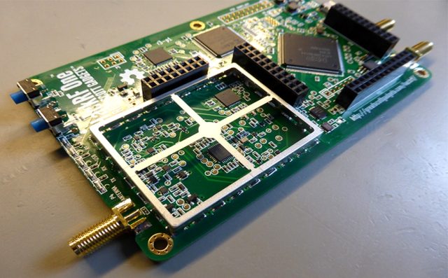
An RF Transceiver PCB is a specialized circuit board that supports the integration of radio frequency transmission and reception circuits within a single hardware platform.
Modern wireless devices rely on RF transceivers to convert baseband signals into radio signals for transmission, while simultaneously receiving incoming RF signals and converting them back into usable data. The PCB must therefore support both high-frequency RF performance and stable mixed-signal operation.
RF transceiver PCBs are widely used in:
-
Wireless communication modules
-
Cellular network infrastructure
-
Smart IoT devices
-
Automotive radar systems
-
Satellite communication terminals
These applications demand PCBs capable of handling GHz-level frequencies while minimizing signal distortion and electromagnetic interference.
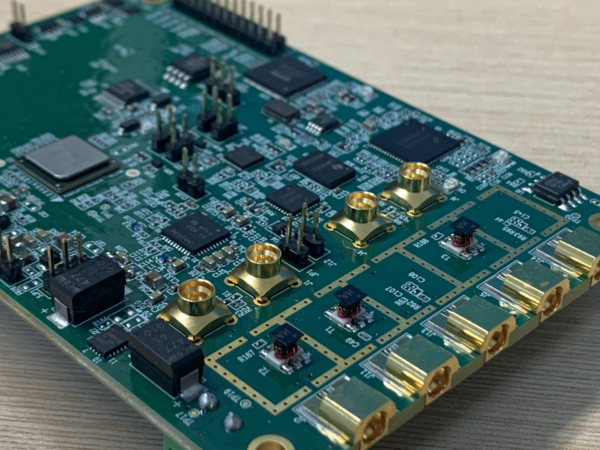
RF Front-End Integration
In many modern wireless systems, the RF transceiver is part of a highly integrated RF front-end architecture. The PCB must accommodate multiple RF components such as:
-
Power amplifiers (PA)
-
Low-noise amplifiers (LNA)
-
RF filters
-
Frequency synthesizers
-
Antenna matching networks
Careful component placement helps maintain short RF signal paths and consistent impedance, which is critical for stable transceiver performance.
Mixed-Signal PCB Layout
RF transceiver boards often combine analog RF circuits with high-speed digital control logic. This creates challenges related to noise coupling and signal interference.
Effective layout strategies include:
-
Physically separating RF and digital sections
-
Using dedicated ground planes
-
Implementing shielding structures
-
Maintaining clean return paths for RF signals
These techniques reduce digital noise interference and maintain the sensitivity of RF receiver circuits.
Antenna Interface and RF Routing
The connection between the RF transceiver and the antenna is one of the most critical parts of the PCB design.
Key design elements include:
-
Controlled impedance RF traces
-
Matching networks for antenna tuning
-
Minimal trace discontinuities
-
Optimized ground referencing
Proper RF routing ensures maximum signal efficiency between the transceiver and the antenna system.
EMI and Signal Isolation
Wireless devices often operate in environments with multiple RF sources. Without proper isolation, interference can degrade system performance.
Design practices used to mitigate EMI include:
-
RF shielding cans
-
Ground stitching vias
-
Guard traces around sensitive RF paths
-
Segregated power supply routing
These techniques help protect RF circuits from external interference and internal signal coupling.
Thermal and Power Considerations
RF transceivers and power amplifiers can generate significant heat during operation. Efficient thermal design improves both performance stability and component lifespan.
Common approaches include:
-
Thermal vias beneath RF chips
-
Copper heat spreading layers
-
Optimized airflow paths in system enclosures
Proper thermal management ensures the RF system maintains stable gain and frequency characteristics.
Applications of RF Transceiver PCB
RF transceiver PCBs are essential components in modern wireless technology, including:
-
5G communication modules
-
Wi-Fi and wireless networking equipment
-
Automotive radar systems
-
Satellite communication terminals
-
Industrial wireless control devices
In these systems, the PCB design directly affects signal quality, transmission efficiency, and overall system reliability.
Conclusion
An RF Transceiver PCB forms the foundation of many wireless communication systems by integrating transmission and reception functions into a compact circuit platform. Through careful RF layout, controlled impedance routing, signal isolation, and thermal optimization, these PCBs ensure reliable high-frequency communication.
As wireless technologies continue to evolve toward higher frequencies, faster data rates, and greater integration, advanced RF transceiver PCB design will remain critical for supporting next-generation communication systems.
