Next-generation 5G router PCB engineering is reshaping the performance limits of consumer and enterprise wireless systems. As 5G routers, gateways, mesh nodes, and outdoor CPE units push into wider sub-6 GHz and emerging FR1/FR2 ranges, the PCB becomes far more than a mechanical carrier—it is the decisive RF medium that determines insertion loss, antenna efficiency, feedline stability, and modulation accuracy.
A true next-gen 5G router PCB platform is defined by how effectively it controls insertion loss across dense RF paths, including band-select filters, impedance-controlled transmission lines, PA output traces, LNA inputs, and multi-branch antenna feed networks. Long RF feedlines inside the router architecture make dissipation a core issue. Low-loss laminates with tightly controlled dielectric constant (Dk) and low dissipation factor (Df) prevent energy absorption and phase distortion, preserving the integrity of high-order 5G waveforms such as 256-QAM, MU-MIMO streams, and OFDMA subcarriers.
Stable dielectric behavior also plays a measurable role in antenna performance. In a 5G router PCB, even minor Dk drift affects the impedance of matching networks, degrading antenna radiation efficiency and reducing EIRP. By using high-frequency PCB materials engineered for ultra-low insertion loss and consistent RF propagation velocity, 5G router PCB platforms maintain low return loss and provide predictable phase alignment for multi-element MIMO antennas. This directly strengthens coverage, uplink sensitivity, and signal reliability in dense indoor environments.
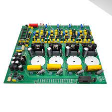
A modern 5G router design integrates 5G modems, Wi-Fi 6E/7 chipsets, switching matrices, beamforming amplifiers, and Ethernet PHYs—all on a compact multilayer PCB. High-density operation introduces thermal loads that influence dielectric behavior. A well-designed 5G router PCB stackup uses thermally stable low-loss laminate systems, thick-copper reference planes, and balanced dielectric spacing to prevent RF detuning caused by temperature-dependent Dk shifts. Stable thermal performance ensures that antenna tuning, insertion loss, and high-frequency impedance remain constant during prolonged high-bandwidth operation.
The evolution toward antenna-on-board (AoB) and antenna-in-package (AiP) architectures places additional demands on the PCB as an RF radiator. Low-loss router PCB substrates reduce conductor losses, dielectric absorption, and parasitic coupling between MIMO channels. These characteristics support higher radiation efficiency, stronger beamforming stability, and more accurate spatial multiplexing—key advantages for routers designed for multi-device environments.
Isolation is equally critical. High-frequency PCB layouts in dual-band or tri-band 5G router designs require strict control of ground plane segmentation, stripline transitions, via stubs, and RF shielding zones. Proper PCB engineering suppresses cross-talk and preserves the low insertion loss characteristics of each RF chain.
Ultimately, next-gen 5G router PCB platforms serve as the electrical, thermal, and RF foundation that enables real-world throughput gains. With reduced insertion loss, optimized impedance control, and enhanced antenna performance, routers achieve higher SNR, greater uplink power, larger indoor coverage radius, and more stable coexistence between5G , Wi-Fi, and Bluetooth subsystems.
These engineering improvements transform the 5G router PCB from a passive carrier into an active RF enabler—supporting multi-gigabit connectivity, latency-critical IoT, and high-density wireless environments.
