Medical diagnostic sensors have shifted toward high-frequency, microwave-based detection architectures to improve resolution, penetration depth, and signal precision. High Frequency Sensor PCB platforms now form the RF backbone of sensing modules used in MRI coils, millimeter-wave tissue scanners, microwave breast-imaging units, vital-sign monitoring radars, and non-contact biomedical sensors.
These RF sensor PCB systems require extremely stable dielectric properties, low insertion loss, controlled impedance, and minimized electromagnetic drift. Small fluctuations in Dk/Df, copper roughness, or layer alignment immediately distort the sensitivity curve and reduce diagnostic accuracy.
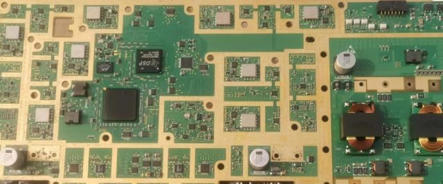
High Frequency Sensor PCB engineering—based on low-loss laminates such as RO4835, RF-35, or ceramic-filled hydrocarbon composites—enables wideband stability from 500 MHz to 40 GHz. Through refined stackup planning, ground referencing, shielding, and hybrid routing, RF sensor PCBs suppress EMI, maintain stable phase response, and ensure consistent microwave field propagation.
For mission-critical medical sensing, stable RF behavior directly translates to more accurate biological parameter detection, reduced false readings, and improved diagnostic image resolution.
Core Engineering Challenges
| Challenge | Root Cause | Impact on High Frequency Sensor PCB |
|---|---|---|
| Electromagnetic Drift | Insufficient shielding, substrate anisotropy | Sensor baseline instability, false positives |
| Wideband Sensitivity Loss | High insertion loss, copper roughness | Reduced detection depth and accuracy |
| Phase Instability | Dielectric fluctuation, lamination skew | Distorted imaging, calibration errors |
| High-Frequency Attenuation | Low-quality laminate, moisture absorption | Degraded RF gain, higher noise floor |
| Crosstalk Between Sensing Channels | Poor ground isolation | Unstable sensor output in multi-element arrays |
High Frequency Sensor PCB engineering must address each limiting factor to maintain precision in medical diagnostic sensors operating across wide RF bandwidths.
Material Science & Dielectric Performance
Medical sensing platforms rely on laminates exhibiting stable Dk/Df, minimal moisture absorption, and extremely low insertion loss.
| Parameter | Typical Value (RO Series / RF-Grade) | Engineering Benefit |
|---|---|---|
| Dielectric Constant (Dk) | 3.38–3.48 ±0.05 | Stable impedance for RF sensor arrays |
| Dissipation Factor (Df) | 0.0020–0.0030 @10 GHz | Low-loss microwave sensing, high SNR |
| Moisture Absorption | <0.05% | Prevents drift in medical environments |
| Thermal Conductivity | 0.6–0.75 W/m·K | Controls heat around sensitive analog front ends |
| Copper Foil Roughness | <1.2 µm | Reduced conductor loss and phase distortion |
| CTE (Z-axis) | 28–55 ppm/°C | Ensures stability under sterilization and reflow |
These RF laminates significantly outperform FR-4 or standard epoxy systems in sensitivity, thermal stability, and high-frequency attenuation.
