Before a semiconductor chip ever reaches packaging, it must first prove itself on the wafer. Engineers run electrical tests directly on the silicon to identify defective dies early in the manufacturing process.
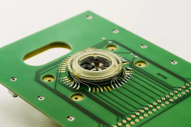
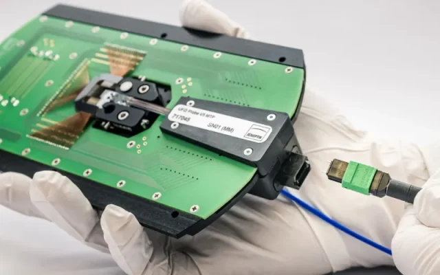
This delicate operation relies on a specialized testing interface known as a Probe Card. At the heart of this system lies the Probe Card PCB, which provides the electrical pathways and structural support needed for accurate wafer-level testing.
Because probe cards operate at extremely fine pitches and often at high frequencies, the PCB design must meet exceptionally strict standards.
What Is a Probe Card PCB?
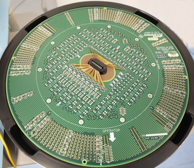
A Probe Card PCB is a high-precision printed circuit board used in wafer testing systems to connect semiconductor testers with probe needles that contact the wafer.
Its main roles include:
• Routing electrical signals between the tester and probe needles
• Maintaining signal integrity for high-speed testing
• Supporting mechanical alignment of probe assemblies
• Handling thousands of repeated test cycles without degradation
The board acts as the electrical backbone of the probe card system.
Key Design Requirements for Probe Card PCBs
Designing PCBs for probe cards pushes PCB engineering to its limits.
Ultra-Fine Pitch Routing
Modern semiconductor wafers may require probe pitches below 50 µm. This means the PCB must support extremely dense routing and microvias.
Signal Integrity
High-speed digital and RF chips demand low-loss signal transmission. Controlled impedance traces and minimal crosstalk are essential.
High Layer Count
Probe Card PCBs often use multilayer structures, sometimes exceeding 20 layers, to handle the large number of signal channels.
Precise Mechanical Stability
The probe card must maintain exact alignment with the wafer pads. Any PCB warping or expansion can affect contact accuracy.
Materials Used in Probe Card PCBs
Materials play a crucial role in electrical performance and mechanical stability.
Common materials include:
High-Tg FR-4
Used for structural stability and thermal endurance.
Low-loss high-frequency laminates
Necessary for high-speed chip testing and RF applications.
Ceramic or hybrid substrates
Sometimes used for ultra-high precision probe cards.
The final material selection depends on the semiconductor node, test frequency, and thermal requirements.
Manufacturing Challenges
Producing a Probe Card PCB is far more complex than standard PCB fabrication.
Challenges include:
• ultra-fine line width and spacing
• high layer alignment accuracy
• microvia reliability
• strict impedance control
Even minor deviations can cause signal distortion or probe misalignment, which leads to inaccurate test results.
Applications of Probe Card PCBs
Probe Card PCBs are essential in multiple semiconductor sectors.
Logic and CPU Chips
Used for wafer-level testing before packaging.
Memory Devices
DRAM and NAND testing require high-channel-count probe cards.
RF and 5G Chips
High-frequency probe cards verify RF performance.
Automotive Semiconductors
Critical chips for vehicles require rigorous wafer testing to meet reliability standards.
Why High-Quality Probe Card PCBs Matter
In semiconductor manufacturing, testing determines yield. A stable and accurate probe card ensures defective chips are identified early while good dies move forward in production.
A well-designed Probe Card PCB enables:
• precise wafer contact
• reliable high-speed signal transmission
• long operational lifespan in testing environments
As semiconductor technology continues to scale down, the demand for advanced Probe Card PCBs will only grow.
