Key Points
-
Definition of the two main concepts of PCB design and manufacturing: class and assembly.
-
Overview of layout department responsibilities: library component creation, component placement, and routing.
-
Detailed explanation of each stage — from receiving the schematic/documentation to generating production files.
Electronic devices have become ubiquitous in the modern world. Whether it’s a device quietly tracking vital signs or a smartphone delivering a constant stream of notifications, a printed circuit board (PCB) lies at the heart of their design. Over the years, PCB manufacturing has continued to evolve to meet the growing demands for newer, faster, and more complex electronic circuits. While an in-depth discussion of PCB design and development could fill an entire library, this article provides a high-level introduction to the fundamentals.
What Is a Printed Circuit Board?
A printed circuit board is a rigid structure containing electrical circuits composed of embedded metallic surfaces known as traces and large metal areas called planes. Components are soldered to the board on metallic pads connected to the circuit traces, allowing the components to interact with each other. A PCB can consist of one, two, or multiple circuit layers.
PCBs are built with a dielectric core possessing low electrical conductivity to ensure clean signal transmission, and may include additional metal and dielectric layers as needed. The standard dielectric material used in PCB fabrication is FR-4, a fire-resistant composite made from woven fiberglass and epoxy resin. The conductive layers—traces and planes—are typically made of copper.
PCB Classes
PCBs are designed for a variety of applications, and one of their distinguishing features is their class — 1, 2, or 3. The class indicates the overall reliability and quality of the board.
-
Class 1 boards are used in consumer electronics.
-
Class 2 boards are used in equipment where high reliability is important but not critical, with a focus on minimizing the likelihood of failure.
-
Class 3 boards follow the strictest standards; their failure could endanger human lives (for example, avionics PCBs).
Types of Printed Circuit Boards
In general, PCBs fall into three main categories: rigid, flexible, or metal-based.
-
Rigid PCBs are the most common and use a stiff substrate laminated under high pressure and temperature. The standard material is FR-4, though variations exist for enhanced performance.
-
Flexible PCBs use bendable materials that can deform significantly, resembling thin film rolls. They are much thinner than rigid boards and are expected to play a major role in future wearable technologies.
-
Metal-core PCBs are a variation of rigid boards that provide enhanced heat dissipation, ideal for high-current applications to prevent thermal damage and failure.
Wherever controlled electromagnetism exists, PCBs form the foundation of the system. Of course, PCBs don’t just appear out of nowhere — their design and manufacturing require extensive engineering expertise.

PCB Design Process
Before a PCB can be manufactured, it must first be designed using CAD tools specifically made for PCB engineering. The design process is typically divided into two main stages:
-
Schematic capture, where the circuit connections are defined, and
-
PCB layout, where the physical board is designed.
Library Component Development
The first step is to develop the necessary CAD library components, which include schematic symbols, simulation models, PCB footprints, and 3D models. Once the libraries are complete, the designer creates the logical schematic, placing and connecting symbols using CAD tools to form the complete circuit.
During this stage, circuit simulation is performed to ensure the design functions as intended. Afterward, net connectivity data is passed from the schematic tools to the layout tools.
Layout
In the PCB layout phase, schematic net data is processed as connections (nets) linking component pins. With the board outline defined, the designer places component footprints in optimal positions. After placement, routing is performed to draw traces and planes connecting the nets.
CAD tools include design rules that prevent trace overlaps and manage widths, clearances, and other parameters. Once routing is complete, manufacturing drawings and output files (Gerber, drill, BOM, etc.) are generated for the fabrication process.
The full design and manufacturing workflow involves:
-
Schematic capture and simulation
-
Design rule setup and DRC verification
-
Component placement
-
PCB routing
-
Power and ground plane design
-
BOM creation and production documentation

How a Printed Circuit Board Is Manufactured
Although PCB design and manufacturing can be summarized as schematic capture → layout → fabrication and assembly, the details of each stage are intricate.
Schematic Creation
Before PCB design begins, all library symbols for components (resistors, capacitors, connectors, ICs, etc.) must be ready. Components are then arranged on schematic sheets, and nets (lines representing electrical connections) are drawn between pins.
Circuit Simulation
With parts and nets organized, SPICE-based simulation tools are used to verify circuit behavior. Simulation allows engineers to test and optimize designs before physical prototyping, saving time and costs.
CAD Tool Setup
Design tools offer many features, including customizable design rules and constraints to ensure proper clearances between nets and objects. Grid systems help maintain neat component placement and trace routing.
Component Placement
Once schematic data is imported, footprints are placed within the board outline. Designers must consider signal integrity, heat dissipation, noise zones, connectors, and mechanical constraints. Component placement must also facilitate efficient assembly during manufacturing.
PCB Routing
After placement, nets are routed using copper traces and planes. CAD tools may include auto-routing features to speed up this process. Designers must ensure correct trace lengths, impedance control, and noise minimization to prevent crosstalk or signal degradation.
Power and Ground Plane Design
Power and ground planes provide current return paths for all active components. Poor plane design — with too many cutouts or voids — can lead to noise and performance degradation. Proper plane continuity is critical for signal integrity.
Final Design Rule Check (DRC)
Once all routing and placements are complete, a final DRC is run. Designers add silkscreen labels, reference designators, dates, and copyrights. Fabrication and assembly drawings are then generated, along with cost estimates.
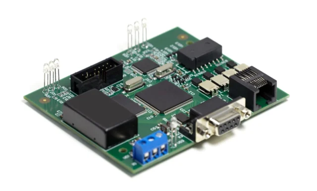
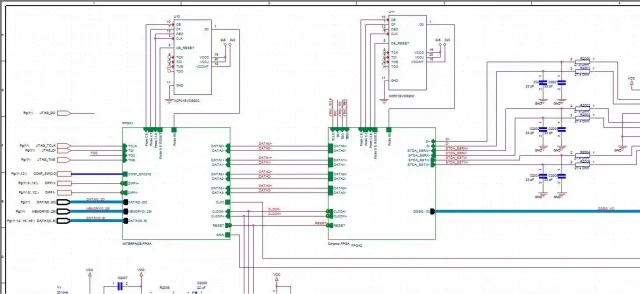
Example: OrCAD PCB Designer
Here’s an example of a PCB layout created using OrCAD PCB Designer.
PCB Fabrication
At this stage, the design is ready for fabrication. Manufacturing involves etching copper traces and planes on each layer and laminating them under heat and pressure to form the final PCB.
During assembly, the board is populated with components and soldered using various processes depending on the component types. The assembled board is then inspected and tested before shipment.
Using PCB Design Tools for High-Quality Results
PCB fabrication and assembly require precision and reliability. Manufacturers depend on accurate design data to produce boards that meet performance expectations.
Advanced PCB design tools must provide powerful features — from high-speed routing and customizable design rules to robust simulation and extensive component libraries. Fortunately, today’s professional PCB design systems, such as Cadence PCB Design Suite, can meet these demands for even the most complex designs.
Leading electronics companies rely on KKPCB products to optimize power, space, and energy requirements across a wide range of market applications.
If you’d like to learn more about our innovative solutions, contact our expert team or subscribe to our YouTube channel.
