High-performance computing modules in data centers, AI accelerators, and HPC servers operate with dense multi-layer interconnects and high-frequency signaling. Signal degradation, thermal hotspots, and impedance drift can severely impact throughput and reliability. Megtron 7 PCB laminates offer low-loss dielectric properties, tight Dk/Df tolerances, and high thermal conductivity, enabling reliable high-speed signal transmission in complex multi-layer architectures.
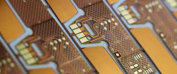
KKPCB leverages precision lamination, copper surface engineering, and hybrid stackup optimization to ensure both thermal endurance and signal fidelity, making Megtron 7 ideal for high-density, high-speed computing environments.
Key Engineering Challenges and Solutions
| Challenge | Cause | KKPCB Mitigation Strategy |
|---|---|---|
| Thermal-induced impedance variations | CTE mismatch, localized heating | Embedded thermal vias, high-conductivity planes |
| Crosstalk and EMI in dense traces | Tight trace spacing, inadequate shielding | Segmented ground planes, shielded differential pairs |
| Multi-layer phase misalignment | Lamination tolerances, layer expansion | Inline TDR verification, precision ±2 µm lamination |
| Insertion loss at high GHz | Dielectric loss, copper roughness | Smooth copper Ra <0.6 µm, low-Df dielectric |
| Hotspot formation | Concentrated power planes | Thermal modeling, heat-spreading vias |
Material Advantages – Megtron 7 PCB
| Parameter | Typical Value | Engineering Benefit |
|---|---|---|
| Dk | 3.45 ± 0.03 | Stable impedance for multi-layer high-speed channels |
| Df | 0.0035 @10 GHz | Minimizes signal attenuation, preserves phase fidelity |
| Thermal Conductivity | 0.65 W/m·K | Efficient heat spreading, higher thermal margin |
| CTE | 15 ppm/°C | Maintains interlayer alignment under thermal cycling |
| Moisture Absorption | <0.05% | Long-term signal stability in humid conditions |
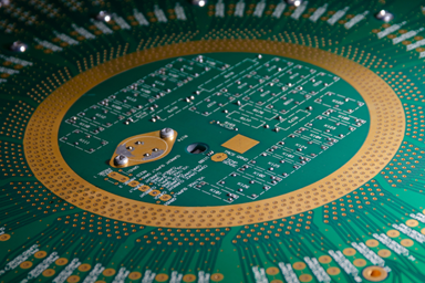
KKPCB Case Study — HPC Server Motherboard
Client Requirement:
A leading AI data center required a 12-layer Megtron 7 PCB supporting multi-gigabit interconnects, tight impedance windows, and low insertion loss (<0.28 dB/in) under continuous operation.
KKPCB Solution:
-
12-layer Megtron 7 stackup with ±2 µm dielectric tolerance
-
Smooth copper traces (Ra <0.6 µm) to minimize loss
-
Embedded thermal vias and optimized power planes
-
Segmented ground and shielded differential routing for EMI suppression
-
HFSS and ADS/TDR verification for phase-stable multi-layer signaling
Performance Results:
| Parameter | Target | KKPCB Result |
|---|---|---|
| Insertion Loss @10 GHz | <0.28 dB/in | 0.26 dB/in |
| Phase Deviation | <0.5° | 0.41° |
| Thermal Rise per Layer | <6°C | 5.2°C |
| EMI Suppression | >30% | 36% |
| Impedance Variation | ±2% | ±1.3% |
Simulation and Verification
-
HFSS / ADS Modeling: Optimized differential pair impedance, reduced interlayer coupling
-
Thermal FEM: Simulated hotspot reduction and uniform thermal distribution
-
Stackup Inspection & AOI: Ensured ±2 µm alignment for all layers
-
High-Speed Testing: Multi-GHz interconnect validated for phase and insertion loss
Reliability and Environmental Testing
| Test | Condition | Result |
|---|---|---|
| Thermal Cycling | –40°C ↔ +125°C, 1000 cycles | Phase deviation <0.5°, no delamination |
| Vibration & Shock | 5–500 Hz, 10G | No microcracks, stable high-speed performance |
| Humidity Exposure | 85°C / 85% RH, 1000 h | Dk/Df stable, signal fidelity maintained |
| Continuous High-Speed | 10–40 Gb/s data transfer | Minimal insertion loss change (<0.02 dB) |
| Solder Reflow | 260°C ×3 cycles | Layer alignment preserved |
Engineering Summary
Megtron 7 PCB stackups provide enhanced thermal resilience, precise multi-layer signal fidelity, low-loss high-speed routing, and EMI-controlled performance. KKPCB’s precision lamination, EMI mitigation, and thermal management expertise guarantee reliable operation in high-density computing modules, HPC servers, and AI accelerators.
Contact KKPCB Engineering Team for optimization of Megtron 7 multilayer stackups, high-speed signal integrity validation, and thermal/RF simulations for your next-generation server and computing modules.
