With the rapid adoption of Wi-Fi 6 and Wi-Fi 7 technologies, laptop wireless modules are operating at higher frequencies, greater data rates, and increased power densities. This evolution introduces new challenges in thermal reliability and electromagnetic interference (EMI) control.
RO4350B PCBs, widely used in high-frequency applications, offer an ideal balance between electrical performance, thermal stability, and manufacturability. However, achieving optimal performance requires careful attention to PCB design, material selection, and layout strategies.
This article explores how to optimize thermal management and EMI suppression in RO4350B-based PCBs for next-generation laptop Wi-Fi modules.
Why RO4350B is Ideal for Wi-Fi 6/7 Applications
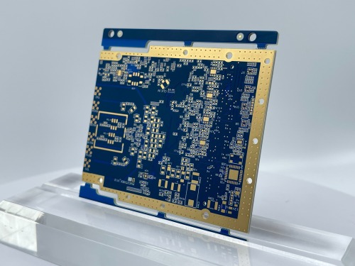
RO4350B is a high-frequency laminate known for its stable dielectric properties and low loss characteristics, making it suitable for RF designs.
Key Advantages:
- Low dielectric loss (Df) → minimizes signal attenuation
- Stable dielectric constant (Dk) → ensures consistent impedance control
- Good thermal conductivity → supports heat dissipation
- Compatible with standard FR4 processing → reduces manufacturing cost
These properties make RO4350B highly suitable for 2.4 GHz, 5 GHz, and 6 GHz (Wi-Fi 6/7) frequency bands.
Thermal Challenges in Laptop Wi-Fi Modules
Despite relatively small form factors, Wi-Fi modules generate significant localized heat due to:
- RF power amplifiers (PAs)
- Baseband processors
- High-speed switching components
Common Thermal Issues:
- Hotspots near RF front-end components
- Reduced performance due to thermal drift
- Long-term reliability degradation
Thermal Optimization Strategies
1. Efficient Stack-Up Design
- Use hybrid stack-ups (RO4350B + FR4) to balance cost and performance
- Place RF layers close to ground planes for heat spreading
- Maintain symmetry to reduce thermal stress
2. Thermal Via Implementation
- Use dense arrays of thermal vias under power components
- Connect to internal ground planes or heat spreaders
- Reduce thermal resistance paths
3. Copper Distribution Optimization
- Increase copper thickness for power traces
- Use copper pours for heat spreading
- Avoid thermal bottlenecks
4. Heat Dissipation Enhancement
- Integrate metal shielding cans as heat spreaders
- Ensure good contact with chassis or heat sinks
- Optimize airflow within laptop enclosure
EMI Challenges in High-Frequency Wi-Fi Design

Wi-Fi 6/7 modules operate at high frequencies and bandwidths, making them more susceptible to EMI issues:
- Signal coupling between RF and digital circuits
- Radiation from high-speed traces
- Interference from nearby components
EMI Control Techniques
1. Proper Grounding Design
- Use continuous ground planes
- Avoid ground splits in RF paths
- Implement via stitching around RF traces
2. Controlled Impedance Routing
- Maintain consistent trace impedance
- Minimize discontinuities
- Use differential pair routing for high-speed signals
3. Shielding Techniques
- Add EMI shielding cans over RF sections
- Use grounded copper areas for isolation
- Separate RF and digital domains
4. Layout Optimization
- Short RF signal paths
- Keep sensitive components away from noise sources
- Optimize return current paths
Balancing Thermal and EMI Performance
Thermal and EMI design goals can sometimes conflict. For example:
- Large copper areas improve heat dissipation but may affect impedance
- Dense via arrays improve thermal conduction but may introduce parasitics
Best Practices:
- Co-design thermal and RF performance
- Use simulation tools for both thermal and electromagnetic analysis
- Validate designs with real-world testing
Manufacturing Considerations
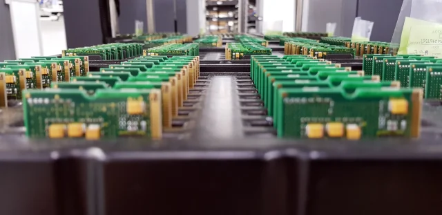
To ensure consistent performance, manufacturers must address:
- Material bonding quality between RO4350B and FR4
- Precision drilling for via integrity
- Surface finish selection (ENIG recommended for RF stability)
- Strict impedance control and testing
Applications
Optimized RO4350B PCBs are widely used in:
- Laptop Wi-Fi 6/7 modules
- Wireless communication cards
- IoT high-frequency devices
- RF front-end modules
Conclusion
As wireless technologies advance, the demand for high-performance, thermally stable, and EMI-resistant PCBs continues to grow. RO4350B provides an excellent platform for Wi-Fi 6/7 modules, but achieving optimal results requires a holistic approach to thermal design and EMI control.
By implementing proper layout strategies, optimization, and advanced manufacturing techniques, engineers can ensure reliable, high-speed wireless performance in modern laptops.
