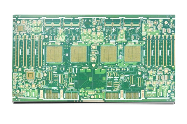
Multilayer PCBs are the backbone of modern electronics, from high-speed communication modules and industrial sensors to automotive and aerospace systems. Before committing to full-scale production, engineers rely on multilayer test PCBs to validate designs, assess signal integrity, and identify potential manufacturing challenges. These test boards simulate the full stack-up of the final product, allowing for comprehensive evaluation under realistic conditions.
Purpose and Design Considerations
-
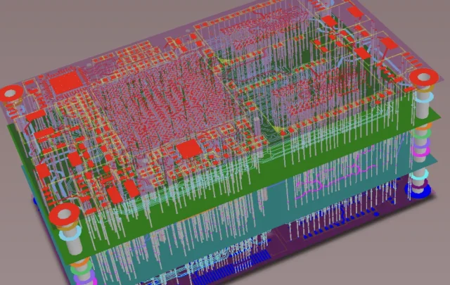
Validation of Layer Stack-Up:
Multilayer test PCBs replicate the final board’s layer structure, dielectric thickness, and material selection. This ensures that the electrical performance of traces, vias, and planes is accurately evaluated before large-scale fabrication. -
Signal Integrity Testing:
High-speed designs require precise control of impedance, differential pairs, and trace routing. Test PCBs allow engineers to measure reflections, crosstalk, and propagation delays, enabling adjustments to stack-up or trace layout before mass production. -
Via and Connectivity Verification:
Blind, buried, and through-hole vias are tested for continuity, plating quality, and reliability. Test PCBs can include intentionally varied via configurations to evaluate process tolerances and optimize manufacturing parameters. -
Thermal and Mechanical Stress Assessment:
Dense multilayer boards are prone to heat accumulation. Test PCBs can incorporate thermal vias, copper pours, and power planes to verify thermal dissipation. Mechanical stress tests simulate bending, vibration, and temperature cycling, ensuring the board withstands operational conditions.
Manufacturing Considerations
Producing multilayer test PCBs closely mirrors full-scale fabrication, often involving:
-
Precise Layer Alignment: Each layer must be accurately registered to prevent shorts or opens.
-
Sequential Lamination: Inner layers are laminated first, with outer layers added in stages to ensure structural integrity.
-
High-Precision Drilling: Vias, microvias, and through-holes must meet strict tolerances for electrical connectivity.
-
Material Verification: Test PCBs use the same substrates and copper thicknesses as final production boards to accurately represent performance.
KKPCB leverages advanced manufacturing capabilities to produce multilayer test PCBs that are representative of final products, ensuring high reliability in evaluation.
Testing and Quality Assurance
Comprehensive testing ensures the validity of multilayer test PCBs:
-
Automated Optical Inspection (AOI): Detects surface defects, misalignment, or incomplete etching.
-
X-ray and Cross-Section Inspection: Verifies internal layers, via integrity, and lamination quality.
-
Electrical Testing: Confirms continuity, impedance, and high-frequency signal performance.
-
Thermal Cycling and Reliability Testing: Validates performance under extreme operational conditions.
Applications of Multilayer Test PCBs
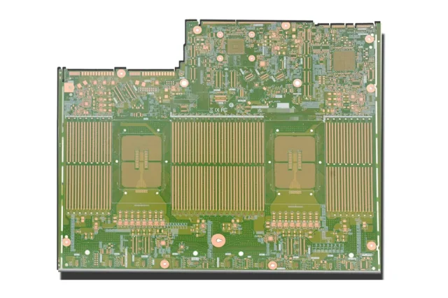
Multilayer test PCBs are widely used in:
-
High-Speed Communication Systems: Validating 5G modules, RF circuits, and networking devices.
-
Automotive Electronics: Ensuring reliability of ADAS, infotainment, and powertrain modules.
-
Aerospace and Defense Systems: Testing high-density, mission-critical electronics.
-
Industrial IoT Devices: Verifying sensors, controllers, and embedded systems before full-scale production.
By thoroughly testing multilayer designs, KKPCB ensures that final production boards meet electrical, thermal, and mechanical requirements. This proactive approach reduces risk, optimizes manufacturing yield, and guarantees performance in demanding applications.
