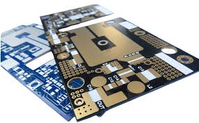
Low Dissipation Factor PCB technology has become essential for next-generation high-frequency, microwave, and mmWave electronic systems. As data rates escalate, carrier frequencies enter the tens of GHz, and RF paths shrink in physical size, signal loss becomes the enemy of performance. Standard FR-4 materials introduce significant dielectric loss, phase distortion, and heat buildup under high-frequency operation.
This is where Low Dissipation Factor PCB—often referred to as Low Df PCB—provides a decisive engineering advantage. With a dielectric loss tangent far below conventional materials, Low Dissipation Factor PCB ensures cleaner transmission, higher signal integrity, reduced attenuation, and superior phase stability across extremely wide bandwidths.
1. Why Dissipation Factor (Df) Defines RF and High-Speed Performance
Dissipation Factor (Df) represents the material’s dielectric loss—how much energy is absorbed and converted to heat. In high-frequency systems, loss grows rapidly as frequency increases.
Low Df PCB materials such as Rogers RO4350B, RO3003, RT/duroid 5880, Megtron 6 deliver:
• Minimal dielectric absorption
• Low insertion loss across microwave and mmWave bands
• Significantly improved power efficiency
• Lower heat rise along transmission lines
• Stable impedance and phase response
These characteristics make Low Dissipation Factor PCB essential for RF front-ends, phased-array antennas, radar, satellite terminals, high-speed backplanes, and any design where loss directly limits performance.
2. Transmission-Line Behavior on Low Dissipation Factor PCB
Transmission-line structures—including microstrip, stripline, grounded coplanar waveguide (GCPW), and hybrid stackups—benefit directly from Low Df PCB materials.
A Low Dissipation Factor PCB reduces:
• Conductor loss due to reduced dielectric heating
• Dielectric loss at high carrier frequencies
• Phase distortion across wideband modulation
• Amplitude imbalance in differential or phased-array networks
• Mode conversion and radiation leakage
In mmWave frequencies (24–86 GHz), the board material’s Df becomes the dominant loss mechanism. Low Df laminates stabilize propagation velocity, enabling precise delay matching for phased-array antennas and beamforming units.
3. Electrical Stability Across Temperature and Humidity
High-frequency systems are notoriously sensitive to environmental variation. Low Dissipation Factor PCB materials deliver exceptional dielectric stability:
• Stable Df over a wide temperature range
• Minimal moisture absorption
• Predictable Dk (dielectric constant) behavior
• Reduced impedance drift under environmental stress
This stability ensures that Low Df PCBs maintain consistent RF performance in harsh conditions:
• Outdoor base stations
• Automotive radar
• Aerospace RF subsystems
• Satellite RF payloads
• High-altitude UAV communication modules
Stable dielectric performance translates directly into reliable system-level behavior.
4. RF Stackup Engineering for Low Df PCB Designs
Stackup design is a critical engineering dimension for Low Dissipation Factor PCB applications. Engineers often combine:
• Low-Df core layers for RF lines
• FR-4 or mid-loss layers for digital circuits
• Hybrid bonding processes for cost optimization
To maintain low-loss performance, stackup engineering must ensure:
• Controlled impedance
• Stable dielectric spacing
• Smooth copper profile for reduced conductor loss
• Isolation between RF, digital, and power planes
• Balanced thermal expansion across laminate types
Advanced bonding films—such as Rogers 2929 bondply—allow seamless integration of Low Dissipation Factor PCB materials into hybrid high-frequency architectures.
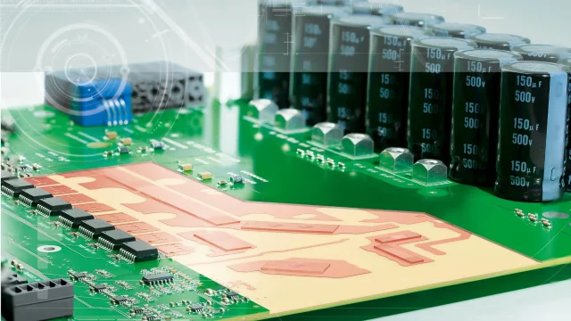
5. Thermal Advantages of Low Dissipation Factor Materials
Low Df PCB materials inherently produce less heat because they waste less signal energy. The benefits include:
• Reduced thermal stress along RF paths
• Lower risk of dielectric breakdown
• Less drift in high-power RF amplifiers
• Better long-term material reliability
Power-sensitive systems such as satellite payloads, radar transmitters, and RF amplifiers gain a significant performance margin when built on Low Df PCB laminates.
6. Application Domains Where Low Dissipation Factor PCB Is Mandatory
Low Df PCB technology is widely deployed in:
• 5G / 6G RF front-end modules
• mmWave automotive radar (76–81 GHz)
• SATCOM terminals and phased-array antennas
• High-speed data channels above 28–112 Gbps
• Microwave filters, couplers, dividers, baluns
• Aerospace and defense microwave electronics
• Precision timing and low-jitter clock distribution
• High-frequency test & measurement equipment
Any system requiring high-efficiency signal propagation, low attenuation, and tight phase control demands Low Dissipation Factor PCB engineering.
Conclusion
The Low Dissipation Factor PCB is no longer a specialized niche material—it is a fundamental enabling technology for high-frequency, high-power, and high-data-rate systems. With ultra-low dielectric loss, stable electrical behavior, and superior thermal efficiency, Low Df PCB materials deliver unmatched signal quality and reliability across RF, microwave, and mmWave applications.
From advanced radar to next-generation base stations and satellite communication platforms, the future of high-frequency electronics relies heavily on Low Dissipation Factor PCB engineering.
