What is a Logic Test PCB?
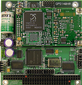
A Logic Test PCB is a printed circuit board specifically created for testing and verifying digital circuits, logic gates, microcontrollers, and complex integrated circuits (ICs). Unlike standard production PCBs, logic test boards are engineered to facilitate troubleshooting, functional testing, and rapid prototyping of digital electronics.
Logic test PCBs are widely used in electronics development, manufacturing validation, and quality assurance processes. They often include multiple test points, jumper pads, and configurable signal paths to accommodate various testing scenarios.
Logic Test PCB Design
Designing a Logic Test PCB requires careful planning to ensure accurate testing and reliable results:
-
Test Point Accessibility:
Test points must be strategically placed for easy access by oscilloscopes, logic analyzers, and automated test equipment (ATE). Clear labeling and spacing help prevent accidental short circuits during testing. -
Signal Integrity Considerations:
High-speed digital signals require controlled trace lengths, proper termination, and impedance matching to prevent signal reflections and glitches during testing. -
Configurable Layouts:
Many logic test PCBs incorporate jumper blocks, switches, or modular connectors to allow rapid reconfiguration for different ICs or logic circuits. This flexibility reduces the need for multiple dedicated boards. -
Power Distribution and Isolation:
Separate power and ground planes for logic circuits minimize interference, while decoupling capacitors stabilize voltage levels during dynamic switching events. -
Component Selection:
Sockets, headers, and test interfaces must withstand repeated insertions and removals without degrading performance. Surface mount or through-hole options are chosen based on testing requirements and mechanical robustness.
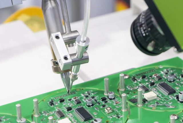
Manufacturing Considerations and QA
Fabrication of logic test PCBs emphasizes durability, precision, and test reliability:
-
Robust PCB Construction: Multiple layers may be used for signal routing, power distribution, and ground isolation. High-quality substrates prevent warping under repeated testing cycles.
-
Durable Finishes: Gold-plated pads, ENIG, or immersion silver finishes improve wear resistance for frequent probing.
-
Precise Assembly: Sockets and test connectors are soldered accurately to avoid intermittent connections.
-
Inspection and Testing:
-
Continuity Checks: Ensure all traces and test points are correctly connected
-
Functional Validation: Boards are pre-tested to confirm compatibility with logic analyzers or ATE
-
AOI/X-ray: Verifies solder joints and component placement
-
KKPCB implements stringent QA processes to ensure that Logic Test PCBs maintain high reliability during repeated testing and diagnostic cycles.
Applications of Logic Test PCBs
Logic Test PCBs are essential in electronics development and production environments:
-
Digital Circuit Validation: Test microcontrollers, FPGAs, and CPLDs before deployment
-
Automated Test Equipment (ATE) Integration: Enable high-speed functional testing for production lines
-
Prototyping and Development: Rapidly evaluate logic circuits during R&D stages
-
Signal Timing Analysis: Debug clocking, propagation delay, and logic gate behavior
-
Quality Assurance: Verify batch consistency and detect manufacturing defects before final assembly
By integrating robust design, flexible layout, precise fabrication, and rigorous QA, KKPCB delivers Logic Test PCBs that enable accurate and reliable validation for modern digital electronics.
