What Is a Logic Test PCB?
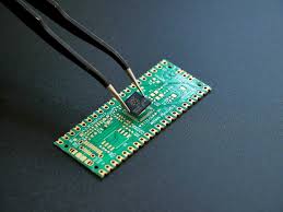
A Logic Test PCB is a specialized printed circuit board designed to verify, debug, and validate digital logic circuits before or during production. It is commonly used to test logic behavior, timing relationships, signal integrity, and functional correctness of digital ICs and systems.
Unlike standard PCBs, a Logic Test PCB focuses on test accessibility, signal stability, and repeatable functional verification, ensuring that digital circuits operate exactly as intended.
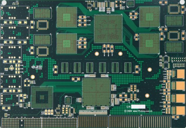
Key Design Considerations for Logic Test PCB
Proper Logic Test PCB design is essential to achieve accurate and repeatable digital testing results. Key considerations include:
-
Clear signal routing
Short, direct traces minimize delay and crosstalk. -
Stable power distribution
Adequate decoupling capacitors ensure clean power for logic devices. -
Test point accessibility
Well-placed test pads support probing and automated test equipment. -
Clock signal integrity
Controlled trace lengths reduce skew and timing errors. -
Grounding strategy
Solid ground planes reduce noise and improve measurement reliability.
These design practices allow Logic Test PCBs to support precise digital logic validation.
Logic Test PCB Manufacturing Requirements
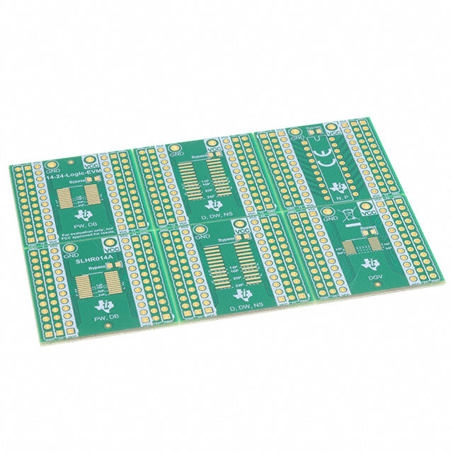
Manufacturing a Logic Test PCB requires consistent quality and tight process control, especially for fine-pitch digital components:
-
Accurate layer registration
-
Consistent trace width and spacing
-
High-quality solder mask alignment
-
Reliable surface finishes (ENIG, OSP, or immersion silver)
-
Electrical continuity and short testing
Reliable manufacturing ensures that the Logic Test PCB does not introduce errors into the testing process.
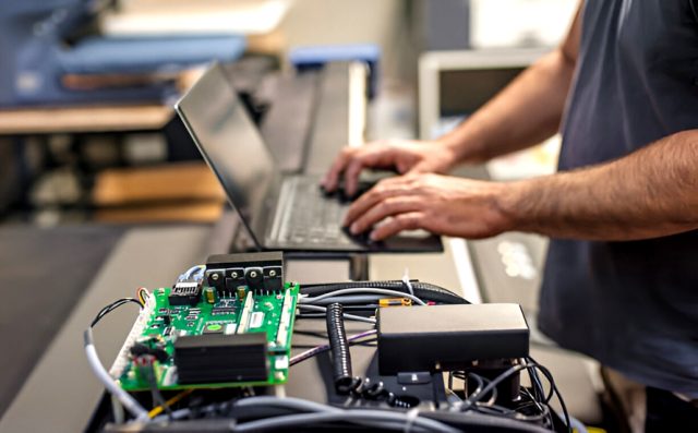
Advantages of Using Logic Test PCB
Using a dedicated Logic Test PCB offers several advantages:
-
Accurate functional verification of digital circuits
-
Repeatable and stable test conditions
-
Faster debugging and fault isolation
-
Reduced risk before mass production
-
Improved overall product reliability
Logic Test PCBs play a critical role in digital system development and validation.
Applications of Logic Test PCB
Logic Test PCBs are widely used in various digital and electronic applications, including:
-
Microcontroller and processor testing
-
FPGA and CPLD validation
-
Digital communication interfaces
-
Industrial control systems
-
Consumer electronics development
-
Automated test equipment (ATE)
Any product involving digital logic can benefit from a Logic Test PCB during development and production.
Logic Test PCB vs. Functional Test PCB
While often used interchangeably, there is a subtle difference:
-
Logic Test PCB focuses on digital logic behavior, timing, and correctness.
-
Functional Test PCB verifies overall system-level functionality.
In practice, many test boards combine both logic testing and functional validation.
Conclusion
A Logic Test PCB is an essential tool for validating digital logic circuits and ensuring reliable electronic system performance. With proper design, quality manufacturing, and clear test objectives, Logic Test PCBs help engineers identify issues early and accelerate product development.
Choosing an experienced PCB manufacturer ensures consistent quality and dependable results for Logic Test PCB applications.
