What Is a Logic Test PCB?
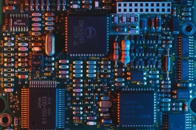
A Logic Test PCB is a specialized printed circuit board used for functional testing and digital logic verification. It is designed to validate logic timing, signal levels, and functional behavior of ICs, modules, and electronic assemblies before mass production.
Logic Test PCBs are widely used in semiconductor ATE systems, functional test fixtures, and production test environments.
Key Requirements for Logic Test PCB
A high-quality Logic Test PCB must meet the following requirements:
-
Stable signal integrity for digital signals
-
Controlled impedance for high-speed lines
-
Low noise and crosstalk
-
Accurate timing and repeatability
-
Reliable connector and socket interfaces
-
Mechanical robustness for repeated test cycles
These characteristics ensure reliable functional test results.
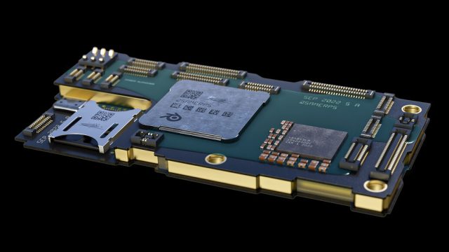
Material Selection for Logic Test PCB
Typical materials used in Logic Test PCB include:
-
High-Tg FR-4
Suitable for most digital logic testing. -
Low-loss FR-4 or hybrid materials
For higher-speed digital signals. -
Heavy copper options
For power-intensive logic test boards. -
Enhanced solder mask and surface finishes
Improve durability and contact reliability.
Material selection depends on signal speed and test conditions.
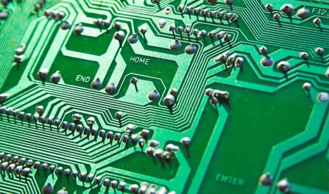
Design Considerations for Logic Test PCB
Effective Logic Test PCB design focuses on:
-
Controlled impedance routing
-
Optimized power and ground planes
-
Short and direct signal paths
-
Proper termination and isolation
-
Minimized skew and timing mismatch
-
Socket, probe, and connector optimization
Good design ensures accurate logic testing and repeatability.
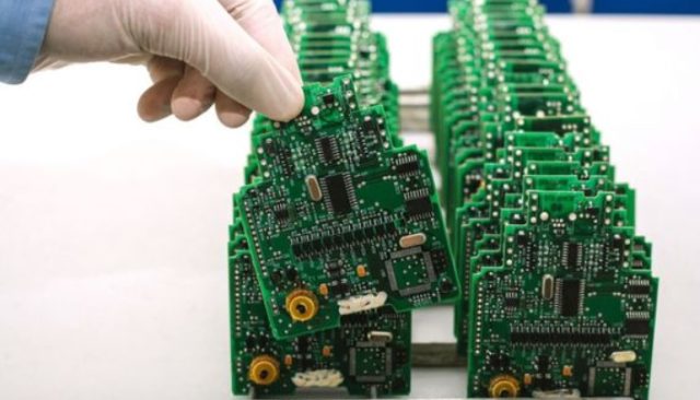
Manufacturing Challenges of Logic Test PCB
Manufacturing a Logic Test PCB requires tight process control:
-
Fine line and spacing accuracy
-
Layer registration and alignment
-
Consistent copper thickness
-
High-reliability via structures
-
Comprehensive electrical testing
Even minor deviations can affect logic test accuracy.
Advantages of Professional Logic Test PCB Manufacturing
Choosing an experienced Logic Test PCB manufacturer provides:
-
High test stability and repeatability
-
Reduced false failures during testing
-
Long service life in production test environments
-
Support for custom logic test fixtures
-
Fast turnaround for prototype and volume orders
These benefits are critical for production and validation testing.
Applications of Logic Test PCB
Logic Test PCBs are commonly used in:
-
Semiconductor functional testing
-
Digital IC and SoC validation
-
ATE and handler systems
-
Production test fixtures
-
Consumer electronics and industrial control testing
-
Automotive electronics functional verification
They play a key role in ensuring correct logic behavior.
Conclusion
A Logic Test PCB is essential for functional and digital logic validation in modern electronics manufacturing. By combining robust design, controlled impedance, and reliable manufacturing processes, Logic Test PCBs deliver accurate, repeatable, and efficient test results.
Working with a qualified Logic Test PCB manufacturer ensures stable performance, high reliability, and consistent quality for logic testing applications.
