What Is a Logic Test PCB?
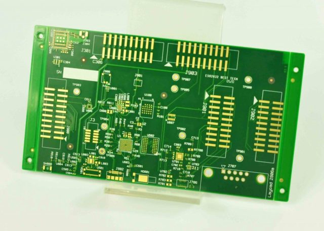
A Logic Test PCB is a specialized printed circuit board used to verify the functionality, timing, and signal integrity of digital logic circuits. Logic Test PCBs are commonly applied in R&D validation, prototype testing, and production testing of digital systems such as microcontrollers, FPGAs, ASICs, and digital interfaces.
Compared with standard PCBs, Logic Test PCBs emphasize testability, repeatability, and measurement accuracy, ensuring digital logic operates exactly as designed.
Key Design Requirements for Logic Test PCB
Reliable Logic Test PCB design is critical to accurate digital testing. Key requirements include:
-
Clean and short signal routing
Minimizes delay, reflection, and signal distortion. -
Stable power distribution network (PDN)
Proper decoupling ensures stable logic levels. -
Clock and timing integrity
Reduces skew and jitter in high-speed digital circuits. -
Accessible test points
Supports probing, debugging, and automated testing. -
Effective grounding and noise control
Solid ground planes reduce EMI and crosstalk.
These design practices directly affect Logic Test PCB performance.
Materials and Manufacturing for Logic Test PCB
Logic Test PCBs typically use high-quality materials and precise manufacturing:
-
High-performance FR-4 laminates
Stable dielectric properties for digital signals. -
Multilayer PCB structures
Supports complex routing and power integrity. -
Surface finishes for repeated testing
ENIG, hard gold, or immersion silver ensure reliable contact. -
Tight fabrication tolerances
Accurate trace width and spacing for consistent logic behavior.
Experienced manufacturers ensure Logic Test PCBs remain stable over repeated test cycles.
Advantages of Using Logic Test PCB
Using a Logic Test PCB offers clear benefits:
-
Accurate verification of digital logic functionality
-
Consistent and repeatable test results
-
Faster debugging and fault isolation
-
Reduced development and production risk
-
Support for high-speed and high-pin-count devices
Logic Test PCBs improve overall product reliability and development efficiency.
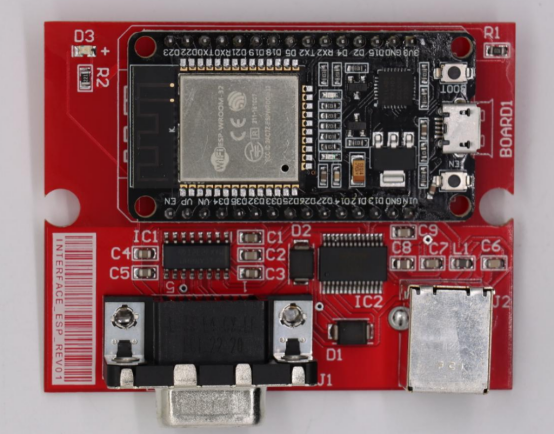
Applications of Logic Test PCB
Logic Test PCBs are widely used in:
-
Microcontroller, FPGA, and ASIC testing
-
Digital interface validation (USB, HDMI, SPI, I²C, etc.)
-
Automated Test Equipment (ATE)
-
Industrial control and embedded systems
-
Consumer electronics functional testing
They are essential wherever digital logic performance must be verified.
Logic Test PCB vs Functional Test PCB
-
Logic Test PCB
Focuses on digital signal behavior, timing, and logic correctness. -
Functional Test PCB
Validates overall system operation under real-use conditions.
Many projects integrate both to achieve comprehensive testing coverage.
Conclusion
A Logic Test PCB is a critical component for accurate digital logic validation and functional verification. Through careful design, high-quality materials, and precision manufacturing, Logic Test PCBs provide stable and repeatable test environments for modern digital electronics.
Choosing an experienced Logic Test PCB supplier ensures reliable test boards that reduce development risk, accelerate debugging, and support high-quality electronic products.
