What Is a Logic Test PCB?
A Logic Test PCB is a specialized printed circuit board designed to verify and validate digital logic circuits during development, prototyping, or production testing. Logic Test PCBs allow engineers to check signal integrity, timing, and functional correctness for digital ICs, microcontrollers, FPGAs, and other logic devices.
Compared with standard PCBs, Logic Test PCBs focus on testability, repeatability, and reliable measurement, ensuring digital systems operate exactly as intended.
Key Design Considerations for Logic Test PCB
Proper Logic Test PCB design is essential for accurate and repeatable testing. Critical design considerations include:
-
Clear signal routing
Short, direct traces minimize delay, reflection, and crosstalk. -
Stable power distribution
Adequate decoupling and proper trace width maintain reliable voltage levels. -
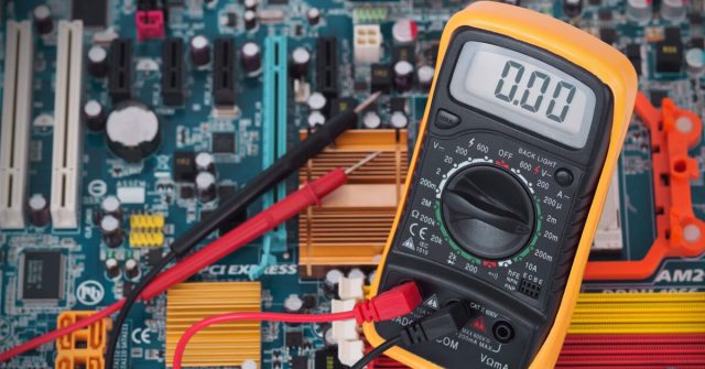
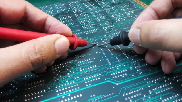
Test point accessibility
Convenient placement of test pads for probing or automated test equipment. -
Clock signal integrity
Ensures timing consistency and reduces skew or jitter. -
Grounding and noise control
Solid ground planes reduce interference during logic testing.
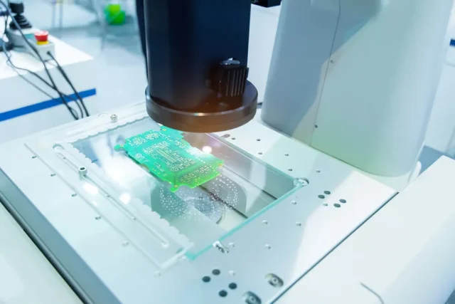
Materials and Manufacturing for Logic Test PCB
To maintain high reliability and accuracy, Logic Test PCBs often require:
-
High-quality FR-4 or hybrid substrates
Ensures consistent electrical performance. -
Precise trace width and spacing
Maintains proper logic levels and reduces signal distortion. -
Surface finishes compatible with repeated testing
ENIG, hard gold, or OSP for reliable probe contact. -
Multilayer or HDI construction
Supports complex digital systems with high pin-count ICs.
Experienced PCB manufacturers ensure Logic Test PCBs can withstand repeated test cycles without degradation.
Advantages of Using Logic Test PCB
Using a Logic Test PCB provides several benefits:
-
Accurate verification of digital circuits
-
Consistent and repeatable test results
-
Faster fault detection and debugging
-
Reduced risk before mass production
-
Support for complex, high-density logic designs
Logic Test PCBs improve design reliability and accelerate time-to-market for digital products.
Applications of Logic Test PCB
Logic Test PCBs are widely applied in:
-
FPGA and microcontroller verification
-
Digital communication and interface testing
-
Automated test equipment (ATE)
-
Industrial control and embedded system validation
-
Consumer electronics prototyping and debugging
They are essential wherever digital logic circuits must be validated before production.
Logic Test PCB vs Functional Test PCB
-
Logic Test PCB
Focuses on digital logic validation, timing, and signal integrity. -
Functional Test PCB
Verifies overall system functionality under real-world operating conditions.
Many test boards integrate both capabilities to provide comprehensive verification of digital systems.
Conclusion
A Logic Test PCB is a critical tool for ensuring digital electronics perform reliably and accurately. From design to manufacturing, careful attention to trace routing, power stability, grounding, and test point placement ensures consistent test results.
Partnering with an experienced Logic Test PCB manufacturer guarantees durable, high-quality test boards that streamline development, improve reliability, and reduce risk in digital product launches.
