In many circuits, the system crystal oscillator operates at a high clock frequency, which produces strong harmonic interference. These harmonics not only propagate through the input and output lines but also radiate through space. Therefore, if the PCB layout of the crystal oscillator is not designed properly, strong spurious radiation problems can easily occur. Once such interference is generated, it is very difficult to eliminate through other means. Hence, the layout of the crystal oscillator and CLK signal traces is extremely important in PCB design.
1. Equivalent Circuit of a Crystal Oscillator
In essence, a crystal oscillator functions like a series RLC circuit.
The equivalent circuit of a crystal oscillator shows a series RLC circuit representing the crystal’s mechanical vibration, paralleled by a capacitor representing its electrical connection. The crystal oscillator operates in a series resonance mode.
Where:
-
R is the equivalent series resistance (ESR)
-
L is the equivalent inductance
-
C is the equivalent capacitance
-
Cp is the parasitic capacitance
2. PCB Layout Design for Crystal Oscillators
As the “heart” of a digital circuit, the crystal oscillator directly affects the system’s stability. The choice and layout of the system clock determine the success or failure of the digital circuit.
Because the quartz crystal inside the oscillator is fragile and can break due to external impact, causing startup failure, mechanical stability and placement reliability should be considered in circuit design. The crystal oscillator should be placed away from the PCB edge and device enclosure whenever possible.
When laying out the crystal oscillator on a PCB, consider the following points:
① Avoid placing the crystal too close to the PCB edge, and ground the crystal case.
Otherwise, it may cause strong EMI radiation. Grounding the metal case can prevent the crystal from radiating outward and also shield it from external interference.
If placement near the edge is unavoidable, route a GND trace around the crystal and add via stitching at intervals to form a grounded enclosure around it.
② Do not route signal traces under the crystal oscillator.
Otherwise, signal traces may couple harmonic noise from the crystal. Ensure a solid ground plane beneath it, and keep the area within 300 mils of the crystal free from routing to prevent interference with other signals, components, and PCB layers.
③ When placing filter components under the crystal, ensure capacitors and resistors follow the signal flow direction.
If not properly arranged, the filtering effect will degrade. The decoupling capacitors should be placed as close as possible to the crystal’s power pin and arranged in descending order of capacitance along the power flow direction.
④ Clock traces should be as short and wide as possible, balancing between trace length and distance from heat sources.
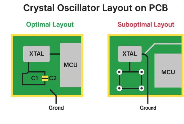
The following layout example shows a better crystal oscillator arrangement:
① The filter capacitors and matching circuit of the crystal are placed close to the MCU, away from the PCB edge.
② The filter capacitors and matching resistors are arranged compactly according to the signal flow direction, close to the crystal.
③ The crystal is placed close to the chip, with traces between them as short and straight as possible.
In any electronic system, high-speed clock signal traces have the highest layout priority. The clock line is a sensitive signal — the higher the frequency, the shorter the routing should be, to minimize signal distortion and ensure system stability.
At KKPCB, we provide comprehensive PCB assembly (PCBA) services combining advanced SMT and DIP assembly lines, full-process quality control, and state-of-the-art testing including X-Ray, AOI, ICT, and functional tests. With extensive experience across medical, consumer electronics, industrial control, and IoT applications, we ensure high-reliability, zero-defect production tailored for custom, small-batch, or lead-free assembly. Our global supply chain, flexible production planning, and integrated ERP/MES/WMS systems guarantee fast, cost-effective, and on-time delivery. Backed by international certifications (ISO, IATF, UL) and strict IPC compliance, KKPCB delivers precision, durability, and consistent performance, supported by 24/7 technical assistance and continuous quality improvement, making us a trusted partner for complex PCB and PCBA solutions worldwide.
