
As electronic devices continue to become smaller, faster, and more powerful, traditional single-sided and double-sided PCBs are often unable to meet modern circuit complexity requirements. Multilayer PCBs have become a key solution for advanced electronic systems by providing higher wiring density, improved electrical performance, and better reliability within a compact footprint.
A multilayer PCB is a printed circuit board consisting of three or more conductive copper layers laminated together with insulating dielectric materials. By integrating multiple signal, power, and ground layers into one structure, multilayer PCBs enable complex circuit designs while maintaining excellent signal integrity and mechanical stability.
Today, multilayer PCB assemblies are widely used in industries such as telecommunications, automotive electronics, medical equipment, industrial control, aerospace, and semiconductor testing.
What Is a Multilayer PCB?
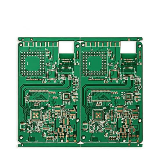
A multilayer PCB is constructed by stacking multiple copper layers separated by insulating dielectric materials, typically prepreg and core materials.
Unlike single-layer or double-layer PCBs, multilayer boards use advanced interconnection technologies, including:
- Through-hole vias
- Blind vias
- Buried vias
- Microvias (for HDI structures)
These technologies allow electrical connections between different layers while maximizing routing density.
A typical multilayer PCB structure includes:
- Signal layers for high-speed and functional routing
- Power layers for stable current distribution
- Ground layers for noise reduction and EMI control
- Dielectric layers for insulation and mechanical support
This layered structure enables designers to achieve higher functionality without increasing PCB size.
Multilayer PCB Manufacturing Process
The manufacturing process of multilayer PCBs requires precise material control, layer alignment, and advanced fabrication technology.
1. Material Selection
The first step is selecting suitable PCB materials according to application requirements.
Common materials include:
- FR-4 for general-purpose applications
- High-Tg materials for high-temperature environments
- Low-loss laminates for high-frequency circuits
- Polyimide materials for flexible and rigid-flex applications
The material selection directly affects:
- Thermal reliability
- Signal integrity
- Mechanical stability
- Manufacturing yield
2. Inner Layer Fabrication
The inner circuit layers are manufactured first.
Main processes include:
- Copper foil preparation
- Dry film lamination
- Photolithography exposure
- Circuit pattern development
- Etching process
- Inspection and repair
The internal copper patterns define signal, power, and ground structures within the multilayer stackup.
3. Multilayer Lamination
After inner layers are completed, multiple PCB layers are stacked together.
The typical structure includes:
- Copper foil
- Prepreg dielectric layers
- Inner core layers
- Additional copper layers
The stacked layers are pressed under controlled temperature and pressure.
During lamination:
- Prepreg resin melts and bonds the layers together
- Copper layers become permanently integrated
- A solid multilayer PCB structure is formed
Precise lamination control is essential to prevent:
- Layer misalignment
- Delamination
- Thickness variation
- Reliability issues
4. Drilling and Via Formation
After lamination, holes are drilled to create electrical connections between layers.
Common via technologies include:
Through-Hole Vias
Connect all layers from top to bottom.
Blind Vias
Connect outer layers to internal layers without passing through the entire board.
Buried Vias
Connect internal layers only.
Microvias
Created by laser drilling and commonly used in HDI multilayer PCBs.
5. Surface Finishing and Testing
The final manufacturing steps include:
- Copper plating
- Surface finishing
- Solder mask application
- Silkscreen printing
- Electrical testing
- AOI inspection
- X-ray inspection
These processes ensure reliable performance and consistent production quality.
Advantages of Multilayer PCBs
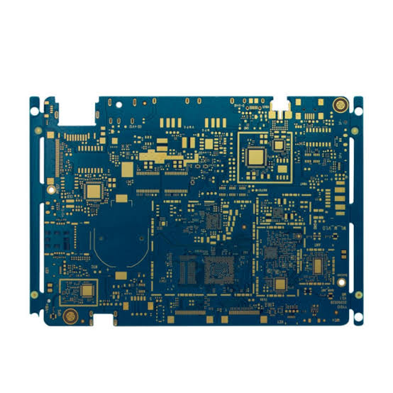
1. Compact Size and High Integration
The biggest advantage of multilayer PCBs is increased circuit density.
Multiple conductive layers allow designers to:
- Reduce PCB size
- Integrate more functions
- Support complex electronic systems
This makes multilayer PCBs ideal for:
- Smartphones
- Wearable devices
- Compact industrial equipment
- Advanced communication systems
2. Improved Electrical Performance
Multilayer structures provide dedicated power and ground planes, improving:
- Signal integrity
- Power stability
- EMI suppression
- High-speed transmission performance
They are especially suitable for:
- High-frequency circuits
- High-speed digital designs
- RF applications
3. Higher Mechanical Reliability
Compared with multiple separate single-layer boards, multilayer PCBs provide:
- Better structural strength
- Improved dimensional stability
- Reduced wiring complexity
The laminated structure helps withstand:
- Mechanical vibration
- Thermal cycling
- Environmental stress
4. Better Space Utilization
By integrating multiple circuits into one board, multilayer PCBs reduce:
- Connector requirements
- Assembly complexity
- System weight
This is important for applications with strict size limitations.
5. Enhanced Current Carrying Capability
Multilayer PCBs can incorporate dedicated power layers and thicker copper structures.
Benefits include:
- Improved current distribution
- Lower voltage drop
- Better thermal management
They are widely used in:
- Power electronics
- Automotive systems
- Industrial control equipment
Challenges of Multilayer PCB Manufacturing
Although multilayer PCBs provide significant advantages, their manufacturing process is more complex.
1. Higher Manufacturing Cost
Compared with single-layer and double-layer boards, multilayer PCBs require:
- More materials
- More processing steps
- Advanced manufacturing equipment
- Strict quality control
Therefore, production costs are higher.
2. Complex Design Requirements
Multilayer PCB design requires professional engineering knowledge in areas such as:
- Stackup design
- Impedance control
- Signal integrity analysis
- Power integrity optimization
- Thermal management
Poor design can result in:
- Crosstalk
- Signal loss
- EMI problems
- Manufacturing difficulties
3. Longer Production Time
Because multilayer PCBs involve multiple fabrication stages, production cycles are generally longer.
Complex designs with:
- High layer counts
- HDI structures
- Fine-pitch routing
require additional processing time and inspection.
4. Higher Manufacturing Capability Requirements
Not all PCB manufacturers can produce advanced multilayer boards.
Reliable production requires:
- High-precision lamination equipment
- Laser drilling capability
- Advanced inspection systems
- Experienced engineering teams
Applications of Multilayer PCBs
Consumer Electronics
Multilayer PCBs are widely used in:
- Smartphones
- Tablets
- Smart watches
- Portable devices
Their compact structure supports high functionality in limited space.
Telecommunications
Communication systems rely on multilayer PCBs for:
- Base stations
- RF modules
- Network equipment
- Satellite communication systems
High-layer PCBs provide stable signal transmission and controlled impedance performance.
Automotive Electronics
Modern vehicles contain numerous electronic systems, including:
- ADAS modules
- Battery management systems
- Vehicle control units
- Infotainment systems
Multilayer PCBs provide reliability under:
- Temperature changes
- Vibration
- Long-term operation
Medical Equipment
Medical devices require reliable and compact electronics.
Applications include:
- Diagnostic equipment
- Monitoring systems
- Imaging systems
- Laboratory instruments
Industrial Control Systems
Multilayer PCBs are used in:
- Automation equipment
- Industrial controllers
- Robotics
- Manufacturing systems
Their durability makes them suitable for demanding environments.
Aerospace and Defense Electronics
High-reliability multilayer PCBs support:
- Avionics systems
- Radar equipment
- Communication devices
- Mission-critical electronics
Semiconductor Test Equipment
Advanced multilayer PCBs are widely used in:
- ATE load boards
- IC test boards
- Probe interface boards
These applications require:
- High-density routing
- Controlled impedance
- Excellent electrical repeatability
How to Select a Multilayer PCB Manufacturer?
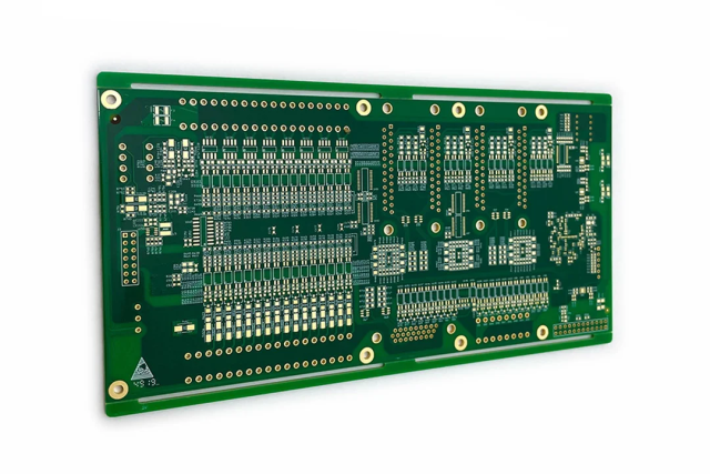
When choosing a multilayer PCB manufacturing partner, key capabilities include:
- High-layer PCB fabrication experience
- Advanced stackup design support
- Controlled impedance capability
- HDI and microvia manufacturing
- High-frequency material processing
- Electrical testing and quality control
- Prototype and volume production support
An experienced manufacturer helps optimize both performance and manufacturability.
Conclusion
Multilayer PCBs have become a fundamental technology for modern electronic systems, enabling higher integration, improved signal performance, and reliable operation in compact designs.
Through advanced stackup design, precision lamination, controlled impedance manufacturing, and strict quality control, multilayer PCB technology supports increasingly complex applications across communication, automotive, industrial, medical, aerospace, and semiconductor industries.
KKPCB provides advanced PCB manufacturing solutions including multilayer PCBs, HDI PCBs, high-frequency PCBs, rigid-flex PCBs, flexible PCBs, thick copper PCBs, buried/blind via boards, and IC carrier boards, supporting customers from PCB design optimization and prototyping to PCB assembly and mass production.
