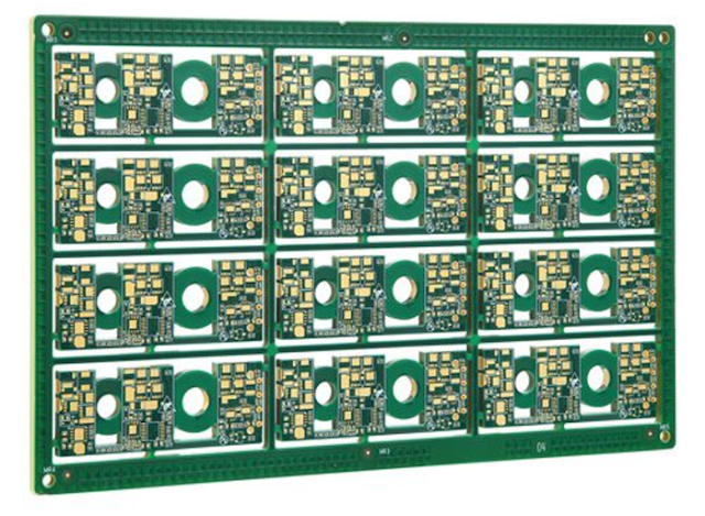
What Is a High Layer Count PCB?

A High Layer Count PCB refers to a multilayer printed circuit board containing a large number of copper layers, typically 12 layers and above, designed to support highly complex circuit routing and high-speed signal transmission.
High Layer Count PCBs are widely used in advanced electronic systems that require high-density interconnection, stable power distribution, and precise signal control.
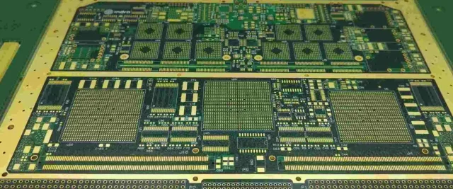
Typical Structure of High Layer Count PCB
A High Layer Count PCB usually includes:
-
Multiple signal routing layers
-
Dedicated ground plane layers
-
Power distribution layers
-
High-performance dielectric materials
-
HDI microvia structures
-
Sequential lamination stack-ups
This complex structure enables efficient signal routing and optimized electromagnetic performance.
Key Technical Advantages
High Layer Count PCBs provide several important benefits:
High Routing Density
More layers allow complex circuit designs with reduced board size.
Improved Signal Integrity
Dedicated ground and power planes reduce noise and signal interference.
Enhanced Power Distribution
Multiple power planes support stable voltage delivery for high-performance processors.
Support for High-Speed Design
Advanced materials and stack-ups help maintain signal performance at high data rates.
Reduced Electromagnetic Interference
Layered ground shielding helps suppress EMI and crosstalk.
Materials Used in High Layer Count PCB
High Layer Count PCBs often require high-performance materials such as:
-
High TG FR-4 laminates
-
Low loss dielectric materials
-
Rogers high-frequency materials
-
Panasonic Megtron series materials
-
Hybrid high-speed material stack-ups
Material selection directly affects signal transmission performance and thermal stability.
Manufacturing Challenges
Producing High Layer Count PCBs requires advanced fabrication technology, including:
Sequential Lamination Process
Multiple lamination cycles ensure structural stability.
Precision Layer Alignment
Tight registration control is required across all layers.
Advanced Drilling Technology
Laser drilling and microvia formation support HDI interconnections.
Thermal Stress Management
Proper material selection prevents delamination during thermal cycling.
Impedance Control and Testing
Accurate impedance verification ensures high-speed signal integrity.
Applications of High Layer Count PCB
High Layer Count PCBs are commonly used in:
-
Data center and server motherboards
-
AI computing and GPU accelerator systems
-
Telecommunications and 5G infrastructure
-
Aerospace and defense electronics
-
Medical imaging and diagnostic equipment
-
Industrial automation control systems
-
Semiconductor test equipment
-
High-performance networking devices
Design Considerations
Engineers designing High Layer Count PCBs must consider:
-
Stack-up symmetry and balance
-
Power integrity and grounding strategy
-
Thermal management design
-
High-speed signal routing techniques
-
Via structure optimization
-
Material compatibility and reliability
Careful design ensures manufacturability and long-term performance.
Conclusion

A High Layer Count PCB is essential for modern electronic systems that require high-density routing, advanced signal integrity, and reliable power distribution. With advanced materials and precision manufacturing technology, High Layer Count PCBs enable complex circuit designs and high-performance electronic applications.
Partnering with an experienced High Layer Count PCB manufacturer ensures consistent quality, accurate impedance control, and reliable production for demanding electronic projects.
