Essential Guide to PCB Testing Methods & Tools
Introduction
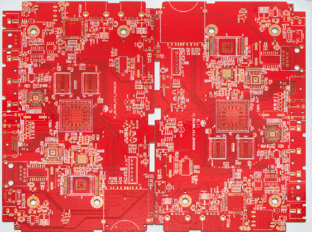
In modern electronics manufacturing, PCB testing is not just a quality step—it’s a reliability guarantee. Testing ensures that every printed circuit board performs exactly as designed, detecting issues such as faulty connections, short circuits, or misplaced components before they reach production.
By identifying problems early, engineers can prevent costly rework, customer returns, and even safety hazards. This article explores the most widely used PCB testing methods, the tools behind them, and best practices to ensure your boards meet the highest quality standards.
Why PCB Testing Matters
Every circuit board, no matter how simple or complex, must undergo thorough testing before it’s ready for use. Even a single weak solder joint or misaligned trace can lead to critical system failures later.
Early-stage testing saves both time and cost—allowing manufacturers to fix defects before scaling production. For industries such as automotive, medical, and aerospace, where safety and reliability are non-negotiable, testing ensures compliance with international standards and guarantees product stability.
Moreover, consistent testing builds brand trust. Fewer failures mean higher customer satisfaction, lower return rates, and a stronger reputation in the marketplace.
What PCB Testing Evaluates
Comprehensive PCB testing covers multiple aspects of both mechanical and electrical integrity, including:
-
Lamination Durability – Ensures internal layers remain bonded under stress or temperature changes.
-
Copper Plating Strength – Verifies that conductive layers can withstand thermal and mechanical strain.
-
Solderability – Evaluates how well solder adheres to pads for long-lasting electrical connections.
-
Hole Wall Reliability – Tests via plating stability across thermal cycles.
-
Electrical Performance – Detects shorts, opens, or resistance issues.
-
Environmental Resistance – Measures performance under humidity, corrosion, or temperature extremes.
-
Cleanliness and Contamination – Ensures no ionic residues remain that could cause long-term failures.
Key PCB Testing Methods
1. In-Circuit Testing (ICT)
ICT is one of the most precise and automated testing methods. Using a bed-of-nails fixture, it checks for shorts, opens, resistance, and capacitance without powering the board.
deal for: High-volume, stable production
Limitation: Requires custom fixtures for each design, adding cost for prototypes.
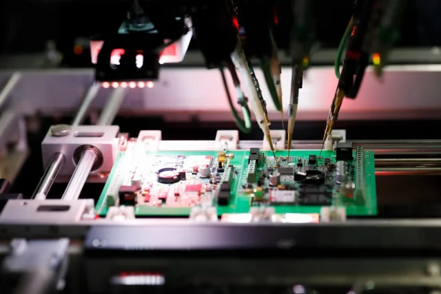
2. Flying Probe Testing
Also known as fixtureless ICT, flying probe systems use movable probes to test each point individually—perfect for small batches or prototypes.
Advantage: No custom fixture, highly flexible
Limitation: Slower than ICT for large-scale production
3. Functional Circuit Testing
This is the final performance validation—powering up the PCB and simulating real working conditions.
Confirms: Full operational readiness
Limitation: Doesn’t identify specific component-level faults.
4. Automated Optical Inspection (AOI)
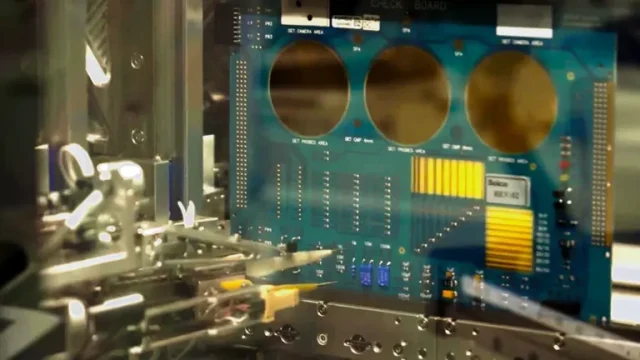
AOI uses high-resolution cameras and image comparison algorithms to detect visual defects like solder bridges, missing components, or polarity errors.
Advantage: Fast, non-contact, ideal for SMT lines
Limitation: Cannot detect internal or electrical issues.
5. X-Ray Inspection (AXI)
AXI provides visibility beneath surface components such as BGAs (Ball Grid Arrays). It’s invaluable for HDI and multilayer PCBs where connections are hidden.
Advantage: Detects hidden voids and cracks
Limitation: High cost and operator skill required
6. Burn-In Testing
Burn-in testing subjects the PCB to elevated temperature and electrical stress for extended periods to expose early failures.
Ideal for: Aerospace, defense, and medical applications
Caution: Excessive stress may shorten product lifespan if overused.
7. Boundary Scan Testing
Used for dense or inaccessible designs, boundary scan sends digital signals through built-in test cells within ICs to verify internal logic paths.
Best for: CPUs, memory, and high-density assemblies
Benefit: No physical probe needed
Additional Testing Techniques
-
Solderability Testing – Verifies solder wetting and adhesion.
-
Peel Strength Testing – Assesses copper layer adhesion.
-
Ionic Cleanliness – Detects contaminants causing corrosion.
-
Micro-section Analysis – Reveals hidden structural defects.
-
TDR (Time-Domain Reflectometry) – Measures impedance and trace continuity.
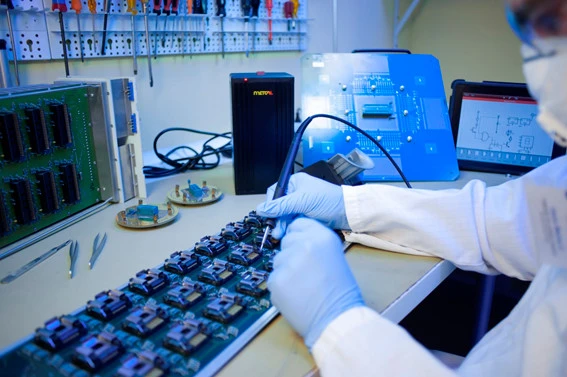
Common Testing Equipment
Bed-of-Nails Tester
Ideal for ICT; it uses thousands of pogo pins to contact test pads simultaneously—fast, repeatable, and accurate for mass production.
Flying Probe Tester
Flexible, fixtureless system ideal for prototyping and low-volume builds.
Automated Test Equipment (ATE)
Combines hardware and software for programmable testing—used for high-volume, automated production lines.
Test Fixtures & Probes
Custom fixtures and pogo pins ensure consistent contact, repeatability, and alignment during testing, improving test reliability.
Design for Testing (DFT)
Design for Testing (DFT) means embedding testability into your PCB layout. Adding test points, probe pads, and accessible traces during design makes later testing faster, cheaper, and more effective.
Integrating DFT with DFM (Design for Manufacturing) and DFA (Design for Assembly) strategies helps optimize yield, assembly, and long-term reliability while reducing rework.
Testing Challenges
-
Miniaturization: Denser boards reduce test access.
-
Speed vs. Accuracy: Fast testing may miss subtle defects.
-
Fixture Costs: Custom setups increase budget for small runs.
-
Technology Evolution: Continuous updates needed for new designs.
Test Planning & Analysis
Structured documentation, calibration schedules, and data tracking form the foundation of effective test management.
Through root cause, statistical, and trend analysis, engineers can identify recurring issues, improve test coverage, and optimize production efficiency.
Conclusion
PCB testing is the cornerstone of reliable electronics manufacturing. By combining multiple testing methods—visual, electrical, and environmental—you can ensure your boards deliver optimal performance under any condition.
At KKPCB, we provide comprehensive PCB fabrication, assembly, and testing services, ensuring each board meets global standards for quality and reliability.
Partner with KKPCB to achieve consistent performance, reduced rework, and total confidence in every circuit you build.
