Automated Test Equipment (ATE) plays a critical role in semiconductor and electronic product validation. At the core of every ATE system is the Custom ATE PCB, a highly specialized test board designed to interface precisely with the device under test and the test platform.
Unlike standard PCBs, custom ATE PCBs are engineered for accuracy, durability, and repeatable performance over extended test cycles.
What Is a Custom ATE PCB?
A Custom ATE PCB is a test-specific printed circuit board developed according to:
-
Test system architecture
-
Device pin count and layout
-
Electrical and mechanical test requirements
Each board is uniquely designed to match a specific ATE platform and test objective.
Why Customization Matters in ATE PCBs
Standardized boards cannot meet the complexity of modern test environments. Custom ATE PCBs enable:
-
Precise signal mapping for high-pin-count devices
-
Optimized power delivery under dynamic loads
-
Mechanical compatibility with sockets, fixtures, and handlers
Customization directly improves test efficiency and yield.
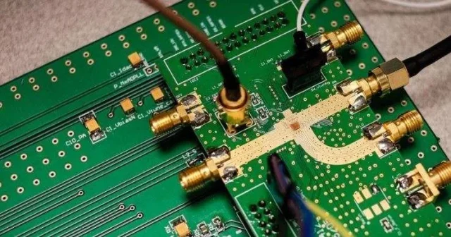
Signal Integrity Requirements in Custom ATE PCBs
ATE systems test devices at high speeds and tight margins. Custom ATE PCBs are designed to:
-
Maintain controlled impedance across all signal paths
-
Reduce crosstalk and noise coupling
-
Minimize skew between parallel test channels
High signal integrity ensures accurate pass/fail decisions.
Power Integrity and Grounding Strategy
Stable power delivery is critical during functional and stress testing. Custom ATE PCBs typically feature:
-
Dedicated power and ground planes
-
Low-inductance decoupling networks
-
Optimized current return paths
These features prevent voltage fluctuation during switching events.
Mechanical Reliability for Repeated Testing
Custom ATE PCBs must withstand:
-
Thousands of test insertions
-
Probe or socket contact pressure
-
Thermal cycling during long test runs
Reinforced pads, robust via structures, and controlled board thickness improve durability.
Stackup Design and Material Selection
Depending on test frequency and environment, custom ATE PCBs may use:
-
High-Tg FR-4 for structural stability
-
Low-loss laminates for high-speed signals
-
Mixed-material stackups for cost-performance balance
Stackup design is tailored to each test scenario.
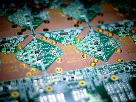
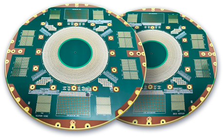
Manufacturing Precision and Quality Control
Custom ATE PCB fabrication requires:
-
Tight layer-to-layer registration
-
Consistent via plating and copper thickness
-
Electrical continuity and impedance testing
Strict quality control ensures repeatable test performance across multiple boards.
Typical Applications of Custom ATE PCBs
Custom ATE PCBs are widely used in:
-
Semiconductor functional testing
-
Parametric and reliability testing
-
Device characterization and validation
-
Production screening environments
Each application demands stable and predictable electrical behavior.
Choosing a Custom ATE PCB Manufacturing Partner
When selecting a custom ATE PCB manufacturer, consider:
-
Experience with semiconductor test boards
-
Engineering support for DFM and test optimization
-
Capability from prototype to volume production
-
Proven quality and traceability systems
A capable partner reduces development risk and test downtime.
Conclusion
A Custom ATE PCB is a critical component of any automated test system. Through tailored design, precise manufacturing, and close engineering collaboration, custom ATE PCBs enable accurate, repeatable, and efficient testing throughout the product lifecycle.
Working with an experienced custom ATE PCB supplier ensures your test platform performs reliably under demanding conditions.
