1. The Foundation of Wireless Intelligence
Bluetooth PCBs form the foundation of wireless connectivity in nearly every modern electronic product. These purpose-built circuit boards combine Bluetooth chips, antennas, and power control systems to enable secure, low-power communication between devices.
In consumer products, they bring wireless audio to life — from headphones and speakers to smart assistants. In industrial environments, they stream real-time data from sensors and machines, enabling smart factories and predictive maintenance.
Pre-certified Bluetooth modules further simplify product development. With integrated chips, antennas, and firmware, these modules reduce RF design complexity and accelerate time-to-market for IoT devices, smart home systems, and health wearables.
2. How Bluetooth PCBs Work
A Bluetooth PCB is a carefully engineered ecosystem. Its Bluetooth chip manages pairing, encryption, and power states, while RF filters eliminate interference from Wi-Fi and cellular networks. Power regulators stabilize the voltage supply, ensuring consistent signal strength even during heavy data transmission.
For instance, a Bluetooth audio PCB in wireless headphones continuously balances low-power idle states and high-bandwidth audio streaming, maintaining signal clarity without draining the battery.
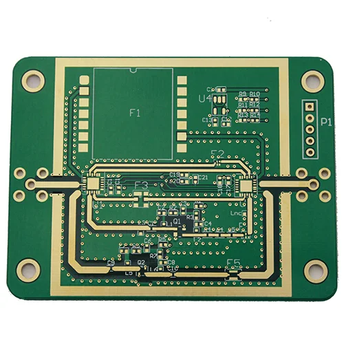
3. Antenna Design and Hardware Integration
The antenna is the heart of wireless performance. Bluetooth PCB antennas are typically designed in two forms:
-
Trace antennas: Cost-effective etched copper traces, ideal for compact devices such as Bluetooth keyboards.
-
Chip antennas: Tiny surface-mount antennas used in space-limited devices like earbuds or health monitors.
Proper impedance matching (usually 50Ω) and isolation from metallic parts minimize signal loss. Supporting hardware — such as RF filters, decoupling capacitors, and voltage regulators — maintains data integrity, ensuring stable transmission even in RF-heavy environments.
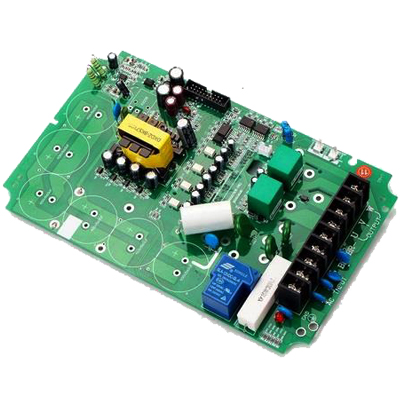
4. Precision Manufacturing at KKPCB
At KKPCB, each Bluetooth PCB is engineered with precision — from material selection to final assembly.
-
Material Engineering: We use FR-4 for cost-effective consumer applications and Rogers or high-Tg substrates for high-frequency, low-loss industrial designs.
-
Layer Management: Dedicated RF, power, and digital layers are separated to prevent electromagnetic interference.
-
Automated SMT Assembly: High-precision machines place micro-scale Bluetooth chips and RF components, ensuring accuracy and consistency across every production batch.
Each board undergoes RF performance testing, functional validation, and compliance verification (Bluetooth SIG, FCC, CE). Only qualified boards leave our factory.
5. From Audio to Industry: The Real Applications
-
Consumer Electronics: Bluetooth audio PCBs enable smooth wireless sound for earbuds, smart speakers, and hearing aids.
-
Peripheral Devices: Energy-efficient keyboard PCBs offer long battery life with minimal latency.
-
Industrial IoT & Automotive: Ruggedized boards transfer real-time data in factories and vehicles, ensuring durability under harsh environments.
6. KKPCB: Engineering the Future of Wireless
KKPCB combines advanced RF design knowledge, manufacturing precision, and extensive material expertise to create high-performance Bluetooth PCBs and modules. Our engineering ensures:
-
Stable signal integrity across all environments
-
Optimized antenna placement and RF tuning
-
Scalable mass production with strict QC
At KKPCB, we don’t merely produce boards; we design the architecture of connectivity itself. Our mission is to power the evolution of intelligent, cable-free systems through precision engineering and innovation.
