Balancing Electrical Performance and Manufacturability in Buried Via PCB Structures
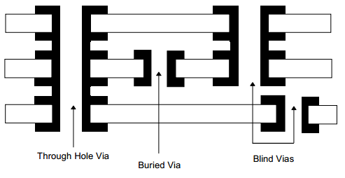
Buried vias are often introduced into PCB designs to improve electrical performance.
Shorter signal paths, reduced stub effects, and higher routing density make buried via PCB structures attractive for high-speed and high-density applications.
In practice, however, electrical optimization and manufacturing stability do not always move in the same direction.
Designs that look excellent in simulation can quickly become difficult—or expensive—to manufacture at scale.
Understanding where this balance breaks is critical for engineers working with buried via PCB structures.
Why Buried Vias Improve Electrical Performance
From an electrical perspective, buried vias offer several clear advantages:
They reduce via stub length, which helps minimize signal reflections in high-speed designs.
They allow cleaner reference plane transitions, improving signal return paths.
They support tighter routing in dense BGA fan-outs without excessive layer count increases.
These benefits are especially valuable in high-speed digital and RF designs, where signal integrity margins are already tight.
However, electrical benefit alone does not define a successful buried via PCB design.
The Hidden Manufacturing Cost of Electrical Optimization
Many buried via PCB issues appear only after manufacturing begins.
Buried vias must be fabricated early in the process and then survive all subsequent lamination cycles.
Each lamination introduces thermal and mechanical stress caused by differences in expansion between copper and dielectric materials.
As buried via density increases or stackups become more complex:
Manufacturing yield becomes more sensitive to small process variations.
Copper plating uniformity becomes harder to control.
The risk of micro-cracks and inter-layer adhesion loss increases.
From a manufacturing standpoint, aggressively optimized electrical designs often push buried via structures closer to their process limits.
When Electrical Performance Conflicts with Manufacturability
Several common design decisions illustrate this conflict.
Reducing via diameter improves electrical performance but narrows the manufacturing window.
Placing buried vias close to impedance-controlled traces can increase stress concentration during lamination.
Minimizing layer count may require additional lamination cycles, increasing cumulative risk.
Each of these decisions may be electrically sound, yet collectively they can degrade manufacturing stability.
Non-Linear Risk in Buried Via PCB Structures
One of the most challenging aspects of buried via PCB design is that risk does not increase gradually.
Below certain thresholds, yield appears stable.
Once stackup complexity, lamination count, or buried via density exceeds a critical point, failures increase rapidly.
This non-linear behavior explains why buried via PCB designs often pass early builds but struggle during volume production.
Practical Guidelines for Engineers
Balancing electrical performance and manufacturability requires early collaboration between design and manufacturing teams.
Engineers should consider:
Whether increasing layer count can reduce lamination cycles.
If slightly larger via diameters can significantly improve yield with minimal electrical impact.
How buried via placement affects both signal integrity and mechanical stress distribution.
Designing with manufacturing limits in mind often results in more robust and predictable performance over the product lifecycle.
A Manufacturing Perspective on Design Trade-Offs
From the factory floor, buried via PCB failures are rarely caused by a single design error.
They are usually the result of multiple marginal decisions stacking together.
Manufacturability is not a constraint imposed after design—it is a design parameter itself.
When electrical performance and manufacturability are balanced early, buried via PCB structures can deliver both high performance and reliable mass production.
Conclusion
Buried via PCB structures offer undeniable electrical advantages, but those advantages must be weighed against real manufacturing constraints.
The most successful designs are not those that maximize electrical performance in isolation,
but those that achieve sustainable electrical performance within stable manufacturing limits.
In buried via PCB design, engineering excellence lies not in pushing every parameter to its extreme,
but in understanding where performance gains no longer justify manufacturing risk.
