The Evolution of Embedded Component Technology in Modern Electronics
Looking back at the evolution of computing—from Apollo workstations and early mainframes to ultrathin laptops and smartphones—the miniaturization of electronic components has always been central to technological progress. As devices become smaller and more powerful, engineers must balance form factor, functionality, PCB materials, signal integrity, power performance, and manufacturing feasibility.
One of the most important breakthroughs pushing this progress forward is embedded component technology, now widely used in aerospace, telecommunications, military applications, medical devices, and consumer electronics.
Why Embedded Component Technology Matters in PCB Design
Driving Miniaturization and Product Innovation
Modern electronics—from compact cameras to wearable health devices—benefit heavily from embedded passive and active components. As production costs decrease, more industries are adopting this technology to create:
-
smaller,
-
faster,
-
higher-functionality,
-
and more energy-efficient devices.
At the same time, printed circuit board (PCB) design and manufacturing have evolved to support these advanced structures.
Evolution of PCB Manufacturing and Embedded Components
Embedded component technology has progressed from simple passive part embedding in laser-cut cavities to high-density multi-layer designs with:
-
high-pin-count ICs embedded inside the substrate,
-
microvias connecting die pads to adjacent conductive layers,
-
electro-optical components with flexible interconnects,
-
polymer-based optical waveguides.
This approach is now a standard process for advanced PCB manufacturers, especially in HDI, substrate-like PCBs (SLP), and system-in-package (SiP) production.
Industry Predictions and the Rise of Embedded ICs
In 2010, IPC market research director Sharon Starr predicted that embedded components would blur the line between PCB fabrication and semiconductor packaging. This proved accurate:
-
PCB production has changed gradually,
-
while wafer-level packaging, chiplets, and SiP technology have advanced dramatically.
Today, embedded components support processors, RF chips, power modules, and memory structures within the PCB stackup.
Benefits of Embedded Component Technology
1. Higher Component Density and Reduced Surface Area
Embedding frees up PCB surface area, allowing more components in the same form factor—critical for mobile phones and wearable devices.
2. Enhanced Electrical Performance
-
Shorter interconnects reduce inductance
-
Higher-speed signals benefit from improved signal integrity (SI)
-
Component shielding can create a Faraday cage effect, reducing EMI sensitivity
3. Thermal and Reliability Improvements
-
Heat dissipation can be integrated into PCB structure
-
Embedded components are less susceptible to mechanical stress or bending
4. Cost Advantages at High Volumes
While PCB cost increases, overall system-level cost may drop due to fewer discrete components and improved assembly efficiency.
5. IP Protection
Embedding complex ICs adds a structural barrier, preventing easy reverse engineering.
Drawbacks and Limitations of Embedded Components
1. Higher Complexity in Design Tools
Traditional 2D PCB tools struggle with embedded component modeling; 3D ECAD systems are required.
2. Manufacturing Tolerance Challenges
Embedded passive components and molded structures require extremely tight tolerances.
3. More Expensive Prototyping
Early iterations have higher costs due to specialized fabrication.
4. Repairability Issues
Embedded devices are nearly impossible to rework after assembly.
5. Thermal Management Risks
Improper placement can worsen heat dissipation and thermomechanical reliability.
6. Additional Power Rails for Multi-Die Systems
Using multiple dies increases power distribution complexity.
Common Design Issues in Embedded Component PCB Design
Designing an embedded component PCB shifts engineering from a 2D task to a 3D system-level approach. Challenges include:
-
high-speed signal performance,
-
insufficient understanding of DFM/DFT rules,
-
lack of early thermal and EMI analysis,
-
tight constraints on component height, spacing, and stackup design.
Types of Embedded Components and Methods
1. Bare-Die / Open-Die Embedding
Used in MCM, COB, and high-speed devices.
Benefits include reduced package size, shorter signal paths, and improved thermal performance.
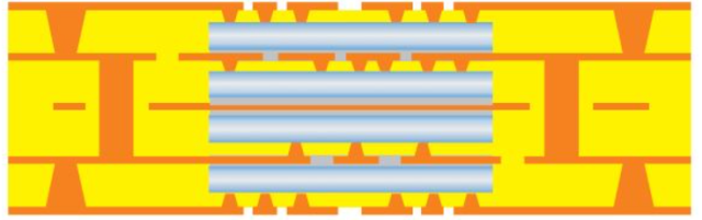
2. 3D Die Stacking (TSV-based SiP)
Stacked dies provide:
-
minimal trace lengths
-
excellent signal rise times
-
reduced inductance
-
improved EMC
This is central to SiP modules used in smartphones, wearables, IoT devices, and miniaturized medical electronics.
Embedding Active Components in PCB Structures
To meet increasing functional requirements in limited space, manufacturers now embed:
-
processors
-
memory
-
custom ASICs
Two main methods are used:
Method 1:Soldering Components Directly onto Inner Layers
Simple but risky—subsequent processing steps may remelt solder.
Method 2:Embedding ICs Between Conductive Layers with Laser Microvias
More advanced:
-
connections formed on both sides
-
minimal footprint
-
supports high-pin-count ICs
-
improved routing and SI
Risk: microvia drilling damage, metallization stress.
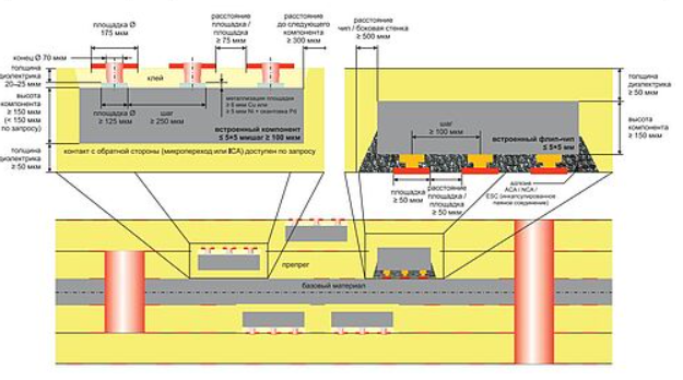
Design Rules for Embedded Components
A robust design environment requires:
-
3D CAD modeling,
-
accurate stackup definitions,
-
cavity structures,
-
microvia constraints,
-
minimum dielectric thickness,
-
interconnect rules,
-
thermal and mechanical requirements.
These rules must align with manufacturing capabilities (HDI, sequential lamination, buildup layers).
Examples include:
-
pad/microvia spacing
-
cavity clearance
-
adhesive wall tolerances
-
component thickness limits
Implementing Embedded Components in a PCB Project
A successful implementation starts at the system architecture stage, involving:
-
3D mechanical design coordination
-
thermal and EMI simulation
-
stackup planning
-
footprint and cavity definition
-
electrical constraint setup
-
collaboration with
Using advanced ECAD tools enables:
-
real-time inner-layer placement PCB manufacturers
-
cavity visualization
-
embedded device modeling
-
automated DRC checks
-
efficient manufacturing output (IPC-2581, ODB++)
Manufacturability and Vendor Collaboration
DFM checks must occur early to avoid costly rework.
Each manufacturer has unique capabilities, so designers must:
-
define fabrication constraints early,
-
validate embedded component rules,
-
perform prototype manufacturing checks,
-
use modern data formats (IPC-2581, ODB++).
Future of Embedded Component Technology
Embedded components enable:
-
ultra-small product footprints
-
higher functionality
-
improved electrical performance
-
integration with advanced packaging (SiP, PoP, SLP)
As manufacturing technologies improve, embedded components will play a central role in next-generation high-density, high-performance, miniaturized electronics.
Early system-level planning and 3D PCB design platforms are essential to fully leverage the benefits of embedded component technology.
