Overview of ADAS PCB in Modern Vehicles
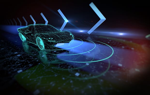
With the rapid development of intelligent vehicles,ADAS PCB has become one of the most critical components in automotive electronics. Advanced Driver Assistance Systems integrate radar sensors, camera modules, LiDAR, ultrasonic detection, and high-performance processors to enable real-time environment perception and decision making.
An ADAS PCB must deliver:
-
High speed data transmission
-
RF signal accuracy
-
Long-term automotive reliability
-
Thermal stability under continuous operation
-
Compact high density integration
Unlike conventional automotive PCB, ADAS PCB supports both high frequency RF circuits and high speed digital processing within a single system.
System Architecture Requirements for ADAS PCB
ADAS systems are typically divided into:
-
Front radar modules
-
Surround camera modules
-
Sensor fusion control boards
-
Central ADAS domain controllers
Each subsystem imposes different PCB design challenges.
Radar Module PCB
Radar modules operating at 24GHz or 77GHz require:
-
Low loss RF laminate
-
Tight impedance tolerance
-
Stable dielectric constant
-
Minimal insertion loss
High frequency material selection directly impacts radar detection accuracy.
Camera and High-Speed Processing PCB
ADAS camera systems transmit large image data streams through:
-
High speed differential pairs
-
Controlled impedance routing
-
Dense BGA breakout
-
Multilayer stack-up structures
Signal integrity design is critical to avoid latency or data distortion.
Core Technical Features of ADAS PCB
1. Hybrid Stack-Up Design
ADAS PCB often uses a hybrid structure combining:
-
High TG FR-4 for digital layers
-
Low loss RF material for radar layers
This configuration balances performance and cost efficiency.
2. High Layer Count & HDI Technology
Modern ADAS domain controllers typically require:
-
8–18 layer PCB
-
Microvia technology
-
Fine line routing
-
High pin count IC support
HDI design ensures compact size while maintaining routing efficiency.
3. Thermal Management Engineering
ADAS processors and radar front-end chips generate significant heat. PCB design may include:
-
Heavy copper planes
-
Thermal via arrays
-
Optimized power distribution networks
-
Metal-backed structures for enhanced cooling
Effective thermal management improves system lifespan.
4. Automotive Reliability Standards
ADAS PCB manufacturing must comply with strict automotive quality systems, including:
-
IATF 16949 process control
-
Full material traceability
-
Thermal cycling validation
-
Vibration resistance testing
Long-term durability is mandatory due to safety-critical applications.
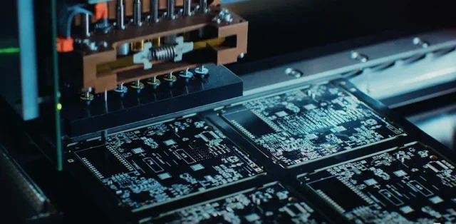
Challenges in ADAS PCB Manufacturing
Producing high quality ADAS PCB involves:
-
Precise impedance simulation and verification
-
Stable multilayer lamination
-
Controlled dielectric thickness tolerance
-
Strict warpage control
-
Electrical and functional testing
Consistency across production batches is crucial for automotive certification.
Future Trends of ADAS PCB
As autonomous driving advances, ADAS PCB will continue evolving toward:
-
Higher frequency mmWave radar
-
Greater data bandwidth
-
Higher integration density
-
Improved EMI shielding
-
Enhanced thermal conductivity
The demand for high performance ADAS PCB is expected to grow significantly in the coming years.
Conclusion
ADAS PCB serves as the foundation of intelligent vehicle safety systems. It integrates high frequency RF performance, high speed signal integrity, automotive-grade reliability, and advanced multilayer design.
A professional ADAS PCB manufacturer ensures optimized stack-up structure, strict quality management, and stable long-term performance for next-generation automotive systems.
