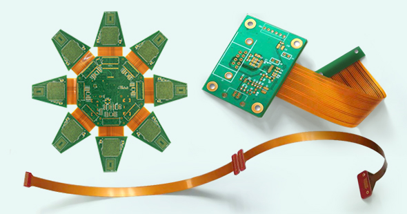
Rigid-flex PCBs combine the flexibility of FPCs with the strength of rigid boards, making them essential in modern electronic devices. Designing high-quality circuits for rigid-flex PCBs requires careful attention to flexible areas, bending zones, and reinforcement materials. This guide explores key challenges and practical solutions for optimal rigid-flex PCB design.
1. Flexible Partition Line Design Considerations
Thickness Transition
In flexible PCB design, sudden thickness changes can cause stress and damage. Use tear-shaped transitions between thick and thin lines to prevent abrupt directional changes.
Corner Treatment
Smooth corners are critical to maintaining circuit stability. Avoid sharp angles to ensure reliable performance, especially in bending areas.
2. Gasket and Pad Design Specifications
-
Maximize gasket size while meeting power transmission requirements.
-
Avoid right-angle transitions between pads and conductors; use smooth curves for better solder joint strength.
-
Independent pads should include solder toes to enhance support and reliability.
3. Ensuring Dimensional Stability
-
Incorporate more copper components, especially in scrap areas, to reduce deformation risk.
-
Plan solid copper bays strategically to improve PCB dimensional stability.
-
Proper copper distribution ensures consistent board quality across rigid-flex sections.
4. Coating Window Design Tips
Manual Alignment Holes
Adding manual alignment holes improves accuracy during the coating process, ensuring precise manufacturing.
Window Size Considerations
Design windows slightly larger than the original to account for adhesive flow. Follow your manufacturer’s ME design standards for exact dimensions.
Special Window Opening Dies
For dense or small windows, use specialized dies like rotary punches or jump punches for precise processing.
5. Rigid-Deflection Transition Zone Design
Line Transition Requirements
Ensure lines transition smoothly in the bending zone. Keep line direction perpendicular to the bending direction to maintain normal circuit operation.
Conductor Distribution Principles
Distribute conductors evenly to avoid dense or sparse regions, reducing stress during bending.
Conductor Width and Process Limitations
-
Maximize conductor width in bending areas.
-
Avoid PTH designs, Coverlays, and non-flowing PP in transition zones to preserve bending performance.
6. Flexible Areas with Air Gap Requirements
-
Through-holes are prohibited in flexible areas to prevent damage.
-
Add protective copper wires on both sides if space permits; otherwise, place them on the inner radius of the bending section.
-
Design circuit connections in an arc shape to accommodate bending.
-
Larger bending areas generally improve flexibility without affecting assembly.
7. Other Key Design Considerations
-
Do not share tool holes on flexible PCBs, including punch holes, ET, and SMT positioning holes.
-
Accurate placement ensures reliable performance in manufacturing.
8. FPC Reinforcement Materials Analysis
PI Reinforcement
-
Tolerance: ±0.03mm
-
High precision and heat resistance (130°C – 280°C)
-
Available thickness: 0.075mm – 0.25mm
-
Pros: small tolerance, high accuracy
-
Cons: insufficient hardness
Steel Plate Reinforcement
-
Thickness: 0.2mm and 1mm
-
Pros: very hard
-
Cons: manual assembly, complex, higher cost
FR4 Reinforcement
-
Thickness: 0.1mm – 1.6mm
-
Tolerance: ±0.05mm (<1mm), ±0.1mm (1mm)
-
Pros: easier than steel to process
-
Cons: larger tolerances at higher thickness
Note: Choose reinforcement materials based on mechanical strength, tolerance, and application requirements for high-quality PCB circuits.
Designing rigid-flex PCBs requires careful consideration of flexible partition lines, gasket and pad specifications, dimensional stability, coating window design, rigid-deflection transitions, bending areas, and reinforcement materials. By following these best practices, designers can ensure high-quality PCB circuits with reliable bending performance and dimensional accuracy.
