The Evolution of Modern PCB Interconnection Technology
As electronic products continue evolving toward:
- smaller size
- lighter weight
- higher functionality
- greater reliability
- compact packaging
traditional PCB structures often struggle to meet modern engineering requirements.
Industries such as:
- aerospace electronics
- medical devices
- military systems
- wearable electronics
- automotive electronics
- robotics
- consumer electronics
increasingly demand PCB solutions capable of:
- three-dimensional integration
- flexible mechanical movement
- high-density interconnection
- compact assembly
- reliable signal transmission
To solve these challenges, engineers widely adopt:
- Rigid-Flex PCB technology
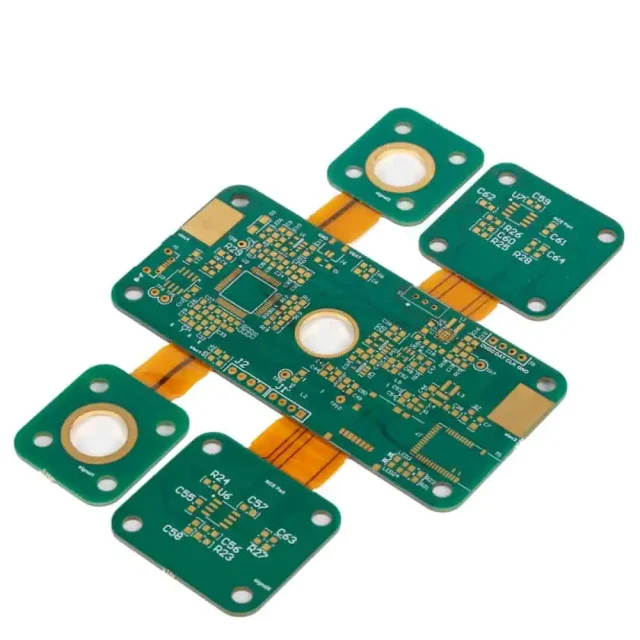
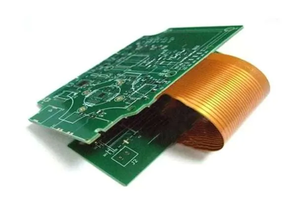
A Rigid-Flex PCB combines:
- rigid PCB sections
with: - flexible PCB layers
within a single integrated circuit board structure.
This hybrid PCB architecture provides:
- compact electronic packaging
- improved reliability
- reduced connector usage
- enhanced mechanical durability
- optimized signal integrity
This article explains:
- rigid-flex layered design
- PCB stack-up structures
- flexible PCB integration
- multilayer rigid-flex PCB fabrication
- design considerations
- advantages
- manufacturing challenges
- industrial applications
What Is a Rigid-Flex PCB?
Definition of Rigid-Flex PCB
A Rigid-Flex PCB is a hybrid printed circuit board structure that integrates:
- rigid PCB layers
and: - flexible circuit layers
into one continuous PCB system.
Rigid sections provide:
- mechanical strength
- component mounting support
- structural stability
Flexible sections allow:
- bending
- folding
- dynamic movement
- compact interconnection
Rigid-flex PCB structures eliminate the need for:
- cable assemblies
- board-to-board connectors
- multiple wiring harnesses
Basic Structure of Rigid-Flex PCB Layered Design
Rigid-flex PCB stackups typically contain:
- rigid copper layers
- flexible copper layers
- dielectric insulation materials
- adhesive systems
- coverlay protection films
The PCB may include:
- multilayer rigid sections
- single-layer flex areas
- multilayer flexible regions
Main Components of Rigid-Flex Layered Design
1. Rigid PCB Layers
Rigid sections are commonly manufactured using:
Rigid layers support:
- IC mounting
- BGA components
- connectors
- power circuits
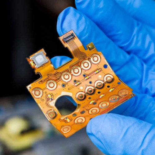
2. Flexible PCB Layers
Flexible layers typically use:
- polyimide materials
Flexible copper circuits enable:
- dynamic bending
- compact folding
- space-saving interconnection
Flex sections are commonly found in:
- cameras
- wearable devices
- medical electronics
- aerospace systems
3. Coverlay Layer
Instead of solder mask, flexible PCB areas use:
- coverlay films
Coverlay provides:
- insulation protection
- mechanical durability
- environmental resistance
4. Adhesive and Bonding Materials
Adhesive systems bond:
- rigid sections
- flex layers
- copper structures
Proper bonding ensures:
- mechanical reliability
- thermal stability
- bending durability
Types of Rigid-Flex PCB Layered Structures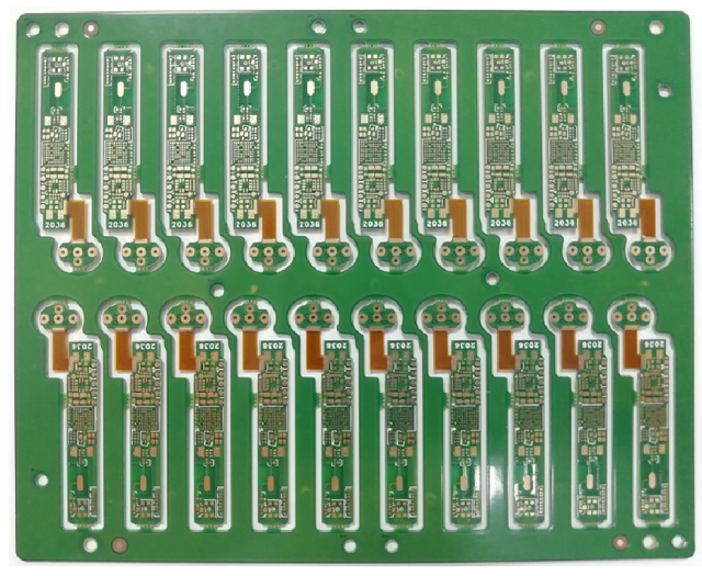
1. Single-Sided Flex with Rigid Sections
Structure:
- one flexible copper layer
- rigid PCB connection areas
Advantages:
- simple structure
- lower manufacturing cost
- flexible routing capability
Applications:
- consumer electronics
- compact portable devices
2. Double-Sided Flexible PCB Structure
Features:
- copper layers on both sides of flex material
Benefits:
- higher routing density
- improved signal capability
- better grounding options
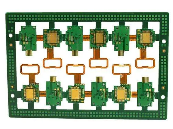
3. Multilayer Rigid-Flex PCB
Combines:
- multilayer rigid PCB
with: - multilayer flexible circuits
Advantages:
- high-density interconnection
- advanced signal routing
- complex system integration
Applications:
- aerospace electronics
- military systems
- medical imaging equipment
4. HDI Rigid-Flex PCB
Advanced rigid-flex PCBs may include:
- microvias
- blind vias
- buried vias
- fine-line routing
Benefits:
- ultra-compact packaging
- high-speed signal routing
- advanced miniaturization
How Rigid-Flex PCB Layered Design Works
The rigid sections:
- provide structural support
- carry mounted components
The flexible sections:
- connect rigid boards
- absorb mechanical movement
- enable folding structures
Electrical continuity is maintained through:
- plated vias
- flexible copper traces
- multilayer interconnections
Advantages of Rigid-Flex Layered Design
1. Space Saving and Miniaturization
Rigid-flex PCB design significantly reduces:
- connector size
- cable requirements
- assembly volume
This enables:
- compact product design
- lightweight electronics
- higher integration density
2. Improved Reliability
Traditional connectors and cables are common failure points.
Rigid-flex PCBs reduce:
- mechanical interconnection failures
- connector fatigue
- wiring problems
Benefits:
- longer product lifespan
- higher vibration resistance
- improved durability
3. Enhanced Mechanical Flexibility
Flexible regions support:
- repeated bending
- folding
- movement
Applications:
- folding electronics
- wearable devices
- robotic systems
4. Reduced Assembly Complexity
Rigid-flex PCB integration minimizes:
- manual wiring
- cable assembly
- connector installation
This improves:
- manufacturing efficiency
- assembly accuracy
- production consistency
5. Better Signal Integrity
Rigid-flex PCBs reduce:
- connector discontinuities
- signal reflection
- EMI coupling
This improves:
- high-speed signal performance
- RF transmission quality
- impedance consistency
6. Weight Reduction
Eliminating connectors and cables reduces:
- system weight
- packaging complexity
Critical for:
- aerospace electronics
- drones
- portable devices
7. Improved Thermal Performance
Rigid copper layers assist:
- heat spreading
- thermal dissipation
- temperature stabilization
Key Design Considerations in Rigid-Flex Layered Design
1. Bend Radius Control
Improper bending may cause:
- copper cracking
- layer delamination
- conductor fatigue
Proper bend radius design improves:
- mechanical reliability
- flex durability
2. Layer Stack-Up Optimization
Rigid-flex stack-up design affects:
- impedance control
- flexibility
- thermal performance
- signal integrity
3. Controlled Impedance Design
High-speed and RF signals require:
- precise impedance control
Important for:
- RF PCB
- high-speed digital PCB
- antenna systems
4. Via Placement Optimization
Avoid placing vias in:
- dynamic bending areas
This reduces:
- mechanical stress
- via cracking risk
5. Copper Balancing
Balanced copper distribution minimizes:
- warpage
- thermal stress
- lamination distortion
6. EMI and Shielding Design
Rigid-flex PCBs often require:
- grounding layers
- EMI shielding
- RF isolation
Especially important in:
- aerospace electronics
- medical equipment
- wireless communication systems
Rigid-Flex PCB Manufacturing Process
1. Flexible Circuit Fabrication
Flex layers are manufactured using:
- polyimide films
- rolled annealed copper foil
2. Rigid PCB Fabrication
Rigid sections are processed similarly to:
- multilayer FR4 PCB manufacturing
3. Lamination Process
Rigid and flex layers are laminated together under:
- controlled heat
- pressure
- alignment conditions
4. Drilling and Via Formation
Mechanical or laser drilling creates:
- interlayer connections
- microvias
- plated through holes
5. Surface Finish and Assembly
Common finishes:
- ENIG
- immersion gold
- immersion silver
Applications of Rigid-Flex PCB Layered Design
Rigid-flex PCB technology is widely used in:
1. Aerospace and Defense
- avionics systems
- satellites
- military communication
2. Medical Devices
- portable medical equipment
- implantable electronics
- imaging systems
3. Consumer Electronics
- smartphones
- cameras
- foldable devices
4. Automotive Electronics
- ADAS systems
- infotainment modules
- sensor integration
5. Industrial Robotics
- robotic arms
- motion control systems
- compact automation modules
6. Wearable Electronics
- smartwatches
- health monitoring devices
- AR/VR systems
Challenges of Rigid-Flex PCB Design
1. Higher Manufacturing Cost
Rigid-flex fabrication is more complex than:
- standard multilayer PCB production
2. Complex Stack-Up Engineering
- flexible regions
- rigid sections
- impedance structures
requires advanced PCB expertise.
3. Mechanical Reliability Concerns
Poor flex design may cause:
- copper fatigue
- delamination
- bending failure
4. Fabrication Complexity
Rigid-flex manufacturing requires:
- precise alignment
- controlled lamination
- specialized processing
Future Trends in Rigid-Flex PCB Technology
1. Ultra-Thin Flexible Electronics
Supporting:
- foldable smartphones
- wearable AI devices
- flexible displays
2. HDI Rigid-Flex PCB
Enabling:
- ultra-high-density routing
- miniaturized electronics
- advanced packaging
3. High-Speed and RF Rigid-Flex PCB
Supporting:
- 5G communication
- aerospace RF systems
- mmWave electronics
4. Advanced Embedded Component Integration
Including:
- embedded passive components
- integrated thermal structures
- embedded shielding
Conclusion
Rigid-flex layered design represents one of the most advanced technologies in modern PCB engineering.
By integrating:
- rigid PCB structures
with: - flexible circuit technology
engineers can achieve:
- compact electronic packaging
- enhanced reliability
- improved signal integrity
- reduced assembly complexity
- lightweight system integration
Rigid-flex PCB technology is essential for:
- aerospace electronics
- medical devices
- automotive systems
- wearable technology
- advanced communication equipment
As electronics continue evolving toward:
- smaller size
- greater flexibility
- higher integration
- advanced RF capability
rigid-flex PCB layered design will remain a key solution for next-generation electronic system development.
