Ensuring Low-Loss Transmission and Thermal Reliability Through KKPCB’s Duroid 5880 PCB Engineering
1. Why Duroid 5880 PCB Defines RF Power Amplifier Reliability
In modern RF Power Amplifier systems used in defense radar, satellite uplink transmitters, and 5G mmWave base stations,
the Duroid 5880 PCB provides exceptional dielectric stability and low-loss performance for power and gain consistency.
Unlike generic PTFE substrates, Duroid 5880 PCBs offer a dielectric constant (Dk = 2.20 ± 0.02) and loss tangent (Df = 0.0009 @ 10 GHz)—essential for maintaining high signal integrity in multi-layer microwave amplifiers.
However, most modern amplifiers require hybrid PCB stackups that integrate Duroid 5880 with RO4350B or FR-4 layers to accommodate bias, control, and ground circuits.
This creates the challenge of achieving perfect dielectric matching and mechanical balance during lamination and RF testing.
2. The Hybrid Stackup Challenge in Duroid 5880 PCB Amplifiers
Hybrid Duroid 5880 PCB stackups combine PTFE-based and hydrocarbon-based materials.
Without precise lamination control, these interfaces can create impedance variation, delamination risk, and thermal stress concentration—especially under high-power RF load.
| Engineering Issue | Cause | Effect on RF Power Amplifier |
|---|---|---|
| Dielectric mismatch | Dk variance between Duroid 5880 and RO4350B | Gain ripple and phase drift |
| Lamination stress | CTE mismatch and uncontrolled resin flow | Microvia cracking and warpage |
| Interface voids | Insufficient bond film or uneven pressure | Localized heating and delamination |
KKPCB’s hybrid stackup methodology ensures the Duroid 5880 PCB maintains both RF precision and thermal integrity across the full multilayer amplifier system.
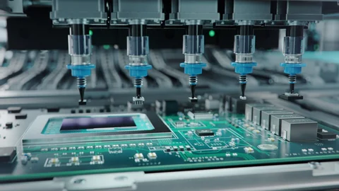
3. KKPCB’s Hybrid Stackup Engineering Workflow
3.1 Material Selection & Layer Balancing
-
Outer RF layers: Duroid 5880 PCB cores (0.254 mm) for ultra-low insertion loss.
-
Inner signal/control layers: RO4350B dielectric to enhance structural rigidity and via reliability.
-
Balanced Z-axis expansion: < 17 ppm/°C for stable thermal cycling.
3.2 Lamination Simulation & Process Control
-
Controlled lamination: 175 °C / 60 min / 200 psi, minimizing resin flow variance.
-
3D FEA simulation validates interlayer stress in hybrid Duroid 5880 PCB stackups.
-
Tolerance across 6-layer amplifier boards: < ±12 µm, ensuring impedance control within ±5 Ω.
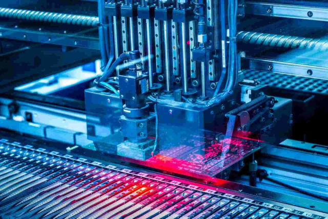
3.3 RF Verification & Reliability Testing
-
Inline VNA/TDR measurement up to 70 GHz validates phase alignment.
-
Cross-section microscopy confirms void-free bonding at PTFE interfaces.
-
Long-term reliability verified under 1000-cycle thermal shock (–55 °C ↔ +150 °C).
4. Case Study — 8-Layer Ku-Band Power Amplifier Using Duroid 5880 PCB
Client: Aerospace communication OEM
Application: 14–18 GHz high-power amplifier for satellite uplink module
PCB Stackup: Hybrid Duroid 5880 + RO4350B multilayer architecture
Design Highlights
-
Dual-core Duroid 5880 PCB structure for the RF transmission layer.
-
Integrated thermal via network under transistor flange area.
-
Hybrid lamination optimization using KKPCB proprietary simulation matrix.
| Metric | Target | KKPCB Result |
|---|---|---|
| Insertion loss @15 GHz | < 0.25 dB/in | 0.21 dB/in |
| Phase drift (–55~+125 °C) | < 1.5° | 0.9° |
| Warpage | < 0.15 mm | 0.11 mm |
| Delamination defects | < 1 % | 0 % |
Result: KKPCB’s Duroid 5880 PCB solution delivered excellent phase stability and thermal uniformity,
enabling the customer’s amplifier to achieve consistent EIRP output and gain linearity during environmental validation.
5. Thermal Management in Duroid 5880 PCB Amplifiers
Thermal dissipation remains critical for RF Power Amplifier reliability.
KKPCB’s hybrid Duroid 5880 PCB architecture integrates:
-
Copper-filled thermal vias to spread heat evenly across the PTFE interface.
-
Low-roughness copper foil (<0.8 µm Ra) to minimize dielectric loss.
-
Dual-bond film control for stable Z-axis conductivity.
These features ensure thermal resistance < 0.35 °C/W and eliminate hot-spot induced gain compression in high-power radar or space-borne amplifiers.
6. KKPCB Reliability Validation Framework
| Test Type | Duration | Result (Duroid 5880 PCB) |
|---|---|---|
| Thermal cycling | 1000 cycles | No delamination |
| 85/85 humidity test | 1000 h | Df drift < 0.0001 |
| Power aging @18 GHz | 500 h | Insertion loss stable |
| Mechanical stress test | 250 mm panel | Warpage < 0.12 mm |
KKPCB validates each Duroid 5880 PCB amplifier stackup through real-world reliability mapping to guarantee field-ready performance.
7. Conclusion — KKPCB’s Engineering Edge in Duroid 5880 PCB Stackups
KKPCB’s hybrid Duroid 5880 PCB stackup design framework enables:
-
Low-loss RF transmission with consistent impedance.
-
Thermal and mechanical balance across multilayer PTFE-hydrocarbon interfaces.
-
Stable performance for aerospace, defense, and mmWave power amplifiers.
With this approach, KKPCB turns Duroid 5880 PCBs into a production-grade platform for precision RF power amplification.
