From High-Frequency Design to Production-Ready Stackups
As next-generation RF systems evolve toward 24–77 GHz applications—such as automotive radar, 5G base stations, and satellite communication—engineers require PCB materials that deliver low loss, thermal stability, and consistent manufacturability.
Rogers RO4835 PCB has become the preferred substrate for these applications due to its low dissipation factor (0.0037 @ 10 GHz), stable dielectric constant (Dk = 3.48 ± 0.05), and enhanced oxidation resistance, ensuring long-term reliability in harsh thermal environments.
However, most production designs today employ hybrid stackups—combining RO4835 with FR-4, low-Dk prepregs, or ceramic cores. These mixed-material structures balance RF precision and cost but require precise lamination engineering to manage CTE mismatch, resin compatibility, and impedance drift.
That’s where KKPCB’s hybrid lamination process control transforms high-frequency design challenges into scalable, production-ready RF systems.
Why Hybrid Stackups Are the Industry Standard
A pure RO4835 PCB stackup ensures dielectric accuracy but increases cost and rigidity.
By contrast, hybrid configurations strategically use RO4835 for RF-critical layers while FR-4 or low-Dk prepregs manage power and control signal routing.
| Layer | Material | Function |
|---|---|---|
| Top | RO4835 (0.254 mm) | RF microstrip / antenna layer |
| Core | FR-4 / Low-Dk Prepreg | Power & control layer |
| Bottom | RO4835 (0.508 mm) | Feed / phase control layer |
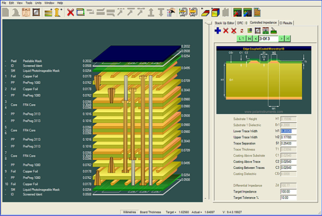
This structure provides the best performance-to-cost ratio, but introduces thermal and mechanical challenges that must be controlled through accurate lamination parameters and stackup symmetry.
Key Lamination Challenges — and KKPCB Solutions
(1) CTE Mismatch Between RO4835 and FR-4
RO4835’s in-plane CTE (≈ 11 ppm/°C) differs significantly from FR-4 (≈ 17 ppm/°C), creating mechanical stress during thermal cycling that can cause warpage or delamination.
KKPCB Process Control
-
Balanced press layup to equalize expansion
-
Vacuum-assisted lamination (< 2 °C/min heating ramp)
-
Real-time thermal mapping for flatness consistency
(2) Resin Flow and Prepreg Compatibility
The ceramic-filled RO4835 resin behaves differently from FR-4. Improper resin flow leads to voids, dry zones, or dielectric spacing variation, causing impedance drift.
KKPCB Process Control
-
Rogers-approved 4450F bonding film or matched low-Dk prepreg
-
Resin-flow simulation to predict squeeze-out
-
Plasma / micro-etch activation for stronger bonding
(3) Impedance Drift & Dielectric Thickness Variation
At mmWave frequencies, even ±10 µm of dielectric variation can shift impedance by 5–8 %.
-
± 5 µm etching precision for conductor geometry
-
Inline VNA impedance verification (≤ 110 GHz)
-
Post-lamination dielectric validation for each batch
(4) Voids & Delamination in Multi-Material Layers
Differences in surface energy between materials can trap microscopic voids, causing local reflections, RF loss, or thermal fatigue.
-
Multi-stage vacuum lamination + 110 °C / 4 hr pre-bake
-
Stepwise pressure ramping to avoid air entrapment
-
Ultrasonic + optical void inspection for QC
RO4835 PCB
Case Study — 77 GHz Automotive Radar Hybrid Module
A Tier-1 automotive supplier partnered with KKPCB to develop a 77 GHz transceiver PCB using a hybrid RO4835 + FR-4 stackup for cost-efficient mass production.
Design Goals
-
Maintain impedance variation < ± 5 %
-
Prevent delamination under –40 °C ~ +125 °C
-
Limit warpage < 0.15 mm / 250 mm
-
Hybrid stackup: RO4835 + FR-4 core + 4450F bonding film
-
Vacuum lamination: 180 °C / 60 min / 200 psi
-
3D thermal + impedance simulation (IPC-TM-650)
| Parameter | Before Optimization | After KKPCB Process |
|---|---|---|
| Impedance Variation | ± 11 % | ± 3 % |
| Delamination Rate | 6 % | < 0.5 % |
| Panel Warpage | 0.28 mm | 0.12 mm |
Engineering Insight
Initial pilot builds revealed micro-void clusters near via transitions, causing > 10 % impedance drift.
By implementing controlled heating + pre-bake, KKPCB reduced void formation and increased RF yield by 8.7 % across 12 lots.
Design & Process Best Practices
For consistent RF and thermal reliability in RO4835 hybrid stackups, KKPCB recommends:
-
Maintain dielectric symmetry, avoid FR-4 mirroring above RF layers
-
Use Rogers 4450F or equivalent low-flow prepreg
-
Limit total lamination cycles (< 2) to prevent Dk drift
-
Validate Dk/Df stability under actual temperature conditions
-
Conduct cross-section + impedance analysis in pilot runs
KKPCB’s Advanced Hybrid Lamination Control
-
± 3 °C plate temperature uniformity
-
Automated resin-flow & void inspection
-
Real-time VNA impedance verification (≤ 110 GHz)
-
IPC Class 3 / IATF 16949 certified production
-
In-house RF reliability lab for accelerated testing
These capabilities ensure every RO4835 PCB hybrid stackup achieves stable RF performance, tight impedance control, and automotive-grade reliability for radar, aerospace, and 5G systems.
Conclusion — From RF Design to Reliable Mass Production
RO4835 hybrid PCBs combine electrical precision and mechanical flexibility—but require expert control of lamination, resin compatibility, and impedance stability.
Through KKPCB’s hybrid lamination expertise, OEMs can move confidently from engineering prototype → mass production, maintaining low defect rates and stable RF performance.
Ready to Optimize Your RO4835 Hybrid PCB?
KKPCB RF Engineering Team Supports:
-
Custom stackup simulation & Dk validation
-
Lamination profile optimization for volume production
-
RF impedance & thermal reliability testing
Contact KKPCB Engineering Support to discuss your RO4835 PCB project or request a DFM stackup review.
