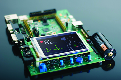
PCB Design for IoT Devices — Challenges and KKPCB Solutions for Compact, Efficient Boards
As the Internet of Things (IoT) reshapes industries—from consumer electronics and healthcare to agriculture—printed circuit boards (PCBs) play a central role in enabling intelligent connectivity. Designing PCBs for IoT devices requires precision, innovation, and balance: compact size, power efficiency, signal integrity, and durability must all coexist in harmony.

At KKPCB, we specialize in advanced PCB design and manufacturing solutions tailored for IoT applications. With years of experience in high-frequency, RF, and multilayer PCB fabrication, our engineering team helps global clients overcome the technical limitations of miniaturization, power management, and wireless integration.
Key Challenges in IoT PCB Design
1. Miniaturization and Space Optimization
IoT devices are often compact and tightly integrated, leaving little room for routing and components. KKPCB engineers employ advanced design-for-manufacturing (DFM) strategies to ensure high functionality within minimal footprints—without compromising reliability or performance.
2. Power Efficiency and Battery Optimization
For IoT devices that rely on long-term battery operation, every milliwatt counts. KKPCB integrates ultra-low-power design principles, using optimized power delivery networks (PDNs), dynamic voltage scaling, and smart sleep-mode circuitry to maximize battery life.
3. Wireless Connectivity and RF Integrity
Stable wireless performance is critical. Our expertise in RF PCB fabrication—including antenna design, impedance control, and mixed-signal integration—ensures superior connectivity for Wi-Fi, Bluetooth, Zigbee, and LoRa systems.
4. Thermal Management for Compact Systems
Heat dissipation is a frequent bottleneck in small IoT devices. KKPCB addresses this through precise copper balancing, thermal vias, and advanced stack-up engineering. Our thermal simulation process minimizes hotspots and extends component lifespan.
5. Signal Integrity and EMI Control
IoT PCBs often operate amid high electromagnetic noise. KKPCB’s strict impedance control, optimized grounding, and EMI shielding techniques guarantee stable, low-noise signal transmission even in densely packed layouts.
6. Durability and Environmental Resistance
IoT devices must endure humidity, vibration, and temperature variation. KKPCB employs durable materials such as Rogers, Isola, and Taconic, complemented by conformal coatings and hybrid stack-ups for long-term reliability in challenging environments.
KKPCB Solutions for Compact, Efficient IoT PCB Design
Multilayer PCB Architecture
KKPCB’s multilayer technology supports complex IoT architectures up to 16 layers, integrating power, ground, and signal planes efficiently. This enables high-density routing while maintaining superior signal integrity and EMI control.
Advanced Power Management Integration
We design PCBs with built-in power optimization—featuring PMICs, low-dropout regulators, and controlled power sequencing—to improve overall efficiency and reduce component count.
Optimized RF and Antenna Design
With in-house RF simulation and testing capabilities, KKPCB provides precision-tuned impedance matching, coplanar waveguide design, and antenna placement services to ensure consistent connectivity across frequency bands from 1 GHz to 77 GHz.
Effective Thermal Engineering
Our engineers apply multi-layer thermal modeling and copper-based heat spreading techniques, ensuring reliable operation for high-density IoT applications such as edge AI or real-time sensor nodes.
Superior Grounding and Shielding
KKPCB applies differential signaling and robust grounding strategies to minimize EMI and crosstalk—ensuring stable performance and compliance with global EMC standards.
Material Science for Reliability
We source and process advanced PCB materials with low dielectric loss, high Tg, and stable Dk/Df characteristics, suitable for flexible and rigid-flex IoT boards alike.
Design Automation and Simulation Tools
KKPCB utilizes the latest EDA and simulation platforms (Altium Designer, Cadence Allegro) for high-precision modeling of signal integrity, thermal dynamics, and manufacturability, ensuring designs move from concept to mass production seamlessly.
Best Practices in IoT PCB Design
-
Component Placement: Logical arrangement for minimal trace length and reduced interference.
-
Trace Routing: Wide power traces and smooth curvature for optimal current flow.
-
Layer Stack-Up: Dedicated planes for power, ground, and signals to enhance EMI performance.
-
Testing & Validation: Each KKPCB design undergoes rigorous testing for signal, thermal, and EMI compliance before delivery.
Future Outlook
Flexible and stretchable PCBs are redefining wearable IoT applications, while SoC and SiP technologies drive further miniaturization. At KKPCB, we’re already investing in AI-driven design automation and next-generation high-frequency substrates, ensuring our clients remain ahead in the connected world.
Conclusion
Designing PCBs for IoT devices is a complex balance of engineering and precision manufacturing. With KKPCB’s expertise in multilayer structures, RF optimization, and material innovation, we deliver compact, efficient, and reliable PCB solutions that empower the next generation of IoT technology.
KKPCB—Advancing IoT Connectivity Through Intelligent PCB Engineering.


