1. Introduction
In the field of high-frequency PCB manufacturing, PTFE-based materials such as Rogers RO3003 and RO4350B are widely used for their low dielectric loss and stable electrical performance.
However, the lamination process for PTFE-based high frequency PCBs is more complex than standard FR4 due to PTFE’s unique mechanical and chemical properties.
This article summarizes key lamination process tips that help engineers and manufacturers achieve consistent quality and stable electrical performance in PTFE laminates.
2. Why Lamination is Critical for PTFE-Based High Frequency PCBs
The lamination process determines the mechanical integrity, dielectric uniformity, and long-term reliability of high-frequency PCBs.
PTFE materials have low surface energy, high thermal expansion, and poor copper adhesion, which means traditional FR4 lamination settings often lead to voids, delamination, or misalignment.
To ensure high yield and consistent RF performance, tight process control and dedicated lamination equipment are required.
3. Key Lamination Process Tips and Parameters
(1) Pre-bake and Material Preparation
-
Pre-bake PTFE cores at 150–180°C for 1–2 hours to remove moisture and stress.
-
Store materials in a dry, temperature-controlled room before use.
-
Plasma treatment before lamination improves adhesion by increasing surface energy.
(2) Bondply and Adhesion Control
-
Choose compatible bondply materials with matching dielectric constants and CTE (e.g., Rogers 2929 bondply).
-
Avoid using FR4 prepregs directly with PTFE cores, as mismatched expansion rates cause delamination under thermal cycling.
(3) Vacuum Lamination
-
Apply vacuum lamination at 370–390°F (190–200°C) under 200–300 psi.
-
Gradual ramp-up and cool-down rates are crucial to avoid trapped air and warpage.
-
Use release sheets and pressure pads to distribute uniform pressure across the panel.
(4) Registration and Alignment
-
PTFE expands more than FR4, so use laser alignment and CTE compensation during tooling design.
-
Maintain registration accuracy within ±25 µm for multilayer high-frequency PCBs.
(5) Post-Lamination Inspection
-
Conduct cross-section analysis to detect voids or resin gaps.
-
Use TDR (Time Domain Reflectometry) and impedance testing to confirm consistency.
-
Inspect for copper peel strength and laminate adhesion to ensure structural reliability.
4. Typical Challenges in PTFE Lamination
| Challenge | Root Cause | Solution |
|---|---|---|
| Delamination | Low adhesion or rapid cooling | Plasma surface treatment + controlled cooling |
| Warpage | CTE mismatch | Use symmetric stack-up & hybrid design balance |
| Void formation | Air entrapment during lamination | Apply vacuum lamination + slow press ramp |
| Misalignment | High expansion rate | Laser registration + CTE modeling |
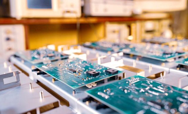
5. KKPCB’s PTFE Lamination Expertise
At KKPCB, we operate dedicated PTFE lamination lines equipped with vacuum hot presses, plasma pre-treatment systems, and temperature-controlled curing environments.
Our engineers optimize each PTFE-based high frequency PCB stack-up according to material type, dielectric thickness, and RF performance requirements.
This ensures excellent signal integrity, impedance control, and mechanical reliability across production runs.
Whether for 24 GHz radar, 5G antenna modules, or satellite communication PCBs, KKPCB provides complete one-stop manufacturing solutions — from material consulting to final electrical testing.
6. Conclusion
The lamination process for PTFE-based high frequency PCBs requires deep understanding of materials, equipment, and process control.
By following precise lamination steps — from pre-bake and plasma cleaning to vacuum lamination and post-test validation — engineers can ensure high reliability and consistent signal performance in every layer.
Partnering with an experienced PCB manufacturer like KKPCB can significantly reduce trial cycles, production risk, and cost while ensuring performance for next-generation RF designs.
