Why PCB Footprint Accuracy Matters
In modern high-speed PCB design, HDI PCB development, and high-density electronic systems, the accuracy of PCB footprints (land patterns) directly impacts:
- Assembly yield
- Solder joint reliability
- Manufacturing efficiency
- Time-to-market
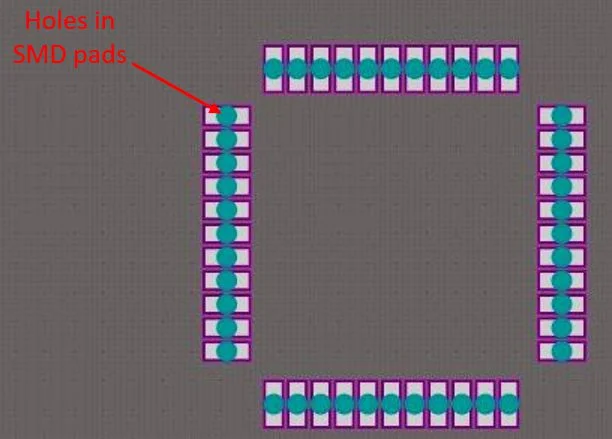
A poorly designed footprint can result in:
- Component misalignment
- Solder bridging or tombstoning
- Rework and production delays
This is why advanced PCB footprint generators have become essential tools for ensuring precision, consistency, and efficiency in PCB design workflows.
At KKPCB, footprint standardization and DFM optimization are key to delivering high-quality PCB and PCBA solutions.
2. What Is an Advanced PCB Footprint Generator?
An advanced PCB footprint generator is a software tool or module that automatically creates component land patterns based on:
- IPC standards (IPC-7351, IPC-2221)
- Component datasheets
- Manufacturer-recommended pad geometries
It enables:
- Automated footprint creation
- Parametric design control
- Consistent library management
- Error reduction in manual design
3. Key Features of Advanced PCB Footprint Generators
3.1 Parametric Footprint Creation
Designers can define:
- Pad size and shape
- Pitch and spacing
- Courtyard and assembly layers
This ensures:
- High accuracy
- Repeatable design standards
- Fast footprint generation
3.2 IPC-Compliant Design
Modern tools follow IPC standards to ensure:
- Manufacturability (DFM)
- Assembly reliability
- Solder joint quality
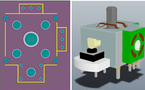
3.3 3D Model Integration
Advanced generators support:
- 3D visualization of components
- Mechanical clearance checking
- Integration with MCAD systems
3.4 Library Management and Standardization
Centralized libraries help:
- Maintain consistency across projects
- Reduce duplication
- Improve team collaboration
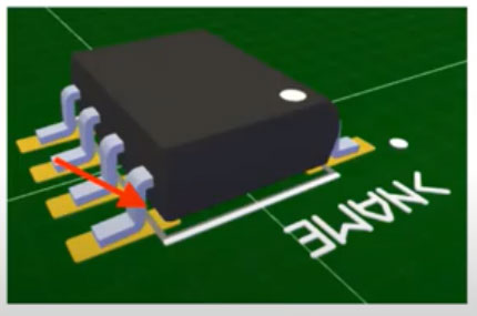
3.5 Automated Error Checking
Footprint generators can detect:
- Pad misalignment
- Incorrect pitch
- Clearance violations
This significantly reduces design errors and rework costs.
4. Benefits of Using Advanced Footprint Generators in PCB Design
4.1 Improved Design Efficiency
Automation reduces:
- Manual drawing time
- Repetitive tasks
- Design cycle duration
4.2 Enhanced Accuracy and Reliability
Accurate footprints ensure:
- Proper solder joint formation
- Reliable electrical connections
- Reduced manufacturing defects
4.3 Faster Time-to-Market
With automated footprint generation:
- Design cycles are shortened
- Prototyping is accelerated
- Product launch timelines improve
4.4 Better DFM and DFA Compliance
Footprints designed with manufacturing rules improve:
- Assembly yield
- Process compatibility
- Production scalability
5. Integration with PCB Design Workflow
Advanced footprint generators integrate with:
- Schematic design tools
- PCB layout software
- Simulation tools
- Manufacturing output (Gerber, ODB++)
They play a central role in:
- Component library creation
- Design rule checking (DRC)
- PCB layout optimization
6. Challenges and Best Practices
6.1 Challenges
- Incorrect datasheet interpretation
- Non-standard component packages
- Library inconsistency
- Over-reliance on automation
6.2 Best Practices
- Verify footprints against manufacturer datasheets
- Maintain a centralized, version-controlled library
- Follow IPC standards strictly
- Validate with DFM checks before production
7. Role in High-Speed and High-Density PCB Design
In high-speed PCB, RF PCB, and HDI designs, footprint accuracy becomes even more critical:
- Fine-pitch components (BGA, QFN) require precise pad design
- Impedance-sensitive routing depends on pad geometry
- Thermal pads affect heat dissipation
Poor footprint design can impact:
- Signal integrity
- Thermal performance
- Assembly reliability
8. KKPCB DFM-Oriented Footprint Engineering Capability
At KKPCB, footprint engineering includes:
- IPC-compliant footprint library development
- DFM/DFA validation before production
- Assembly process optimization
- High-yield PCBA manufacturing support
This ensures:
- Accurate component placement
- Reliable soldering performance
- Efficient large-scale production
9. Future Trends in PCB Footprint Generation
The future of footprint generators includes:
- AI-driven footprint creation
- Cloud-based component libraries
- Real-time DFM feedback
- Integration with digital twins and simulation
These innovations will further enhance PCB design efficiency and accuracy.
10. Conclusion
Advanced PCB footprint generators are a critical tool in modern electronics design, enabling faster, more accurate, and highly reliable PCB development.
By automating footprint creation and ensuring compliance with industry standards, they significantly improve design efficiency, manufacturability, and product quality.
With strong DFM expertise, KKPCB provides optimized PCB solutions that ensure high precision, high yield, and efficient production for global customers.
