
With the continuous development of electronic systems toward higher performance, higher reliability, miniaturization, and harsh-environment operation, traditional PCB technologies face increasing challenges in applications requiring:
- High-temperature resistance
- Excellent electrical insulation
- High-frequency performance
- Long-term reliability
- Compact integration
HTCC (High Temperature Co-fired Ceramic) multilayer substrate technology has become an important solution for advanced electronic packaging and high-reliability circuit applications.
Unlike conventional organic PCB materials, HTCC substrates use ceramic materials that are laminated and sintered at high temperatures, creating a highly stable multilayer structure with excellent mechanical, thermal, and electrical properties.
HTCC multilayer substrates are widely used in:
- Aerospace electronics
- Military and defense systems
- Automotive electronics
- RF and microwave modules
- Semiconductor packaging
- High-temperature sensors
1. What Is an HTCC Multilayer Substrate?
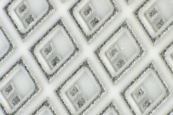
HTCC (High Temperature Co-fired Ceramic) is a ceramic multilayer substrate technology manufactured by stacking and co-firing multiple ceramic layers at high temperatures, typically above 1,500°C.
The basic structure includes:
- Ceramic dielectric layers
- Internal conductive circuits
- Via interconnections
- External metallization layers
During manufacturing, conductive materials are printed onto ceramic green sheets, which are then stacked, laminated, and sintered together to form a compact multilayer circuit structure.
Unlike traditional PCB lamination processes, HTCC creates a ceramic-based integrated structure with:
- High mechanical strength
- High temperature stability
- Excellent insulation performance
2. Main Materials Used in HTCC Substrates
2.1 Alumina (Al₂O₃)
Alumina is one of the most commonly used HTCC materials.
Advantages:
- High mechanical strength
- Excellent electrical insulation
- Good chemical stability
- Mature manufacturing process
Applications:
- Industrial electronics
- Sensor modules
- Power circuits
2.2 Aluminum Nitride (AlN)
Aluminum nitride provides superior thermal performance.
Advantages:
- High thermal conductivity
- Low thermal expansion coefficient
- Excellent heat dissipation capability
Applications:
- High-power semiconductor packaging
- LED modules
- Advanced thermal management systems
2.3 Other Ceramic Materials
Depending on application requirements, HTCC substrates may also use:
- Beryllium oxide (BeO)
- Glass-ceramic materials
Selection depends on:
- Thermal requirements
- Electrical characteristics
- Reliability requirements
3. Manufacturing Process of HTCC Multilayer Substrates
3.1 Ceramic Green Sheet Preparation
The ceramic powder is mixed with:
- Organic binders
- Solvents
- Plasticizers
to form ceramic slurry.
The slurry is processed into thin ceramic sheets called:
Green sheets
These sheets provide the foundation for multilayer fabrication.
3.2 Via Formation
Micro holes are created in ceramic sheets through:
- Mechanical punching
- Laser drilling
These vias provide vertical electrical connections between layers.
3.3 Conductive Pattern Printing
Conductive materials are printed onto ceramic sheets.
Common conductive materials include:
- Tungsten (W)
- Molybdenum (Mo)
- Molybdenum-manganese (Mo/Mn)
The printed patterns form:
- Signal paths
- Power connections
- Ground structures
3.4 Layer Stacking and Lamination
Multiple ceramic layers are aligned and stacked.
During lamination:
- Pressure is applied
- Individual layers are bonded together
High alignment accuracy is required to ensure:
- Reliable interconnections
- Accurate circuit performance
3.5 High-Temperature Co-Firing
The stacked ceramic structure is sintered at high temperatures.
During firing:
- Organic materials are removed
- Ceramic layers become dense
- Conductive patterns form stable internal circuits
This creates a highly reliable multilayer ceramic substrate.
3.6 Surface Metallization and Finishing
After firing, surface processing is performed.
Processes include:
- Metal plating
- Surface finishing
- Component attachment preparation
Common finishes include:
- Gold plating
- Nickel/gold structures
4. Advantages of HTCC Multilayer Substrates
4.1 Excellent High-Temperature Performance
The ceramic structure enables HTCC substrates to operate under extreme temperatures.
Advantages:
- High thermal stability
- Low material degradation
- Reliable operation in harsh environments
Suitable for:
- Aerospace systems
- Automotive engine electronics
- Industrial high-temperature equipment
4.2 Outstanding Electrical Insulation
Ceramic materials provide excellent dielectric properties.
Benefits include:
- High insulation resistance
- Low leakage current
- Reliable high-voltage operation
This makes HTCC suitable for:
- Power electronics
- High-voltage circuits
- Semiconductor packaging
4.3 Excellent Mechanical Reliability
Compared with organic PCB materials, ceramic substrates offer:
- Higher hardness
- Better dimensional stability
- Lower moisture absorption
Advantages:
- Reduced deformation
- Better environmental resistance
- Long service life
4.4 Good High-Frequency Performance
HTCC ceramic materials provide stable electrical characteristics.
Benefits include:
- Low dielectric loss
- Stable dielectric constant
- Reduced signal variation
Applications:
- RF modules
- Microwave circuits
- Communication systems
4.5 Multilayer Integration Capability
HTCC technology enables complex internal structures.
Engineers can integrate:
- Signal layers
- Ground layers
- Power layers
- Passive components
Advantages:
- Reduced package size
- Improved circuit integration
- Better electrical performance
5. Disadvantages and Challenges of HTCC Technology
5.1 Higher Manufacturing Cost
HTCC production requires:
- Ceramic processing
- High-temperature sintering equipment
- Precision manufacturing control
Compared with standard PCB manufacturing, costs are higher.
5.2 Limited Material Processing Flexibility
Ceramic materials are harder than organic materials.
Challenges include:
- Difficult machining
- Higher tooling requirements
- More complex processing
5.3 Longer Development Cycle
HTCC products often require:
- Customized design
- Process optimization
- Reliability validation
This may increase development time.
5.4 Thermal Expansion Matching Requirements
Although ceramic materials have excellent stability, engineers must consider compatibility with:
- Semiconductor chips
- Metal layers
- External components
Incorrect matching may cause:
- Mechanical stress
- Cracking
- Reliability issues
6. HTCC vs Traditional PCB Comparison
| Feature | HTCC Multilayer Substrate | Traditional PCB |
|---|---|---|
| Material | Ceramic | FR-4 / Organic Materials |
| Temperature Resistance | Excellent | Limited |
| Thermal Stability | High | Moderate |
| Electrical Insulation | Excellent | Good |
| High-Frequency Performance | Excellent | Application Dependent |
| Manufacturing Cost | Higher | Lower |
| Mechanical Strength | High | Medium |
| Main Applications | High Reliability Electronics | General Electronics |
7. Applications of HTCC Multilayer Substrates
7.1 Aerospace and Defense Electronics
Requirements:
- Extreme reliability
- Temperature resistance
- Long operational lifetime
Applications:
- Avionics systems
- Radar modules
- Satellite electronics
7.2 RF and Microwave Electronics
HTCC is widely used in:
- RF packages
- Microwave modules
- Antenna systems
Advantages:
- Stable dielectric properties
- Low signal loss
- Precise circuit integration
7.3 Semiconductor Packaging
Applications:
- IC packages
- Power semiconductor modules
- Sensor packaging
Advantages:
- Excellent thermal management
- Reliable electrical connection
7.4 Automotive Electronics
Applications:
- Engine control systems
- Battery management systems
- High-temperature sensors
Advantages:
- Vibration resistance
- Thermal reliability
- Long service life
7.5 High-Temperature Sensors
HTCC substrates are suitable for:
- Gas sensors
- Pressure sensors
- Industrial monitoring systems
Requirements:
- Stable operation under harsh conditions
- Chemical resistance
8. HTCC Design Considerations
8.1 Layer Structure Planning
Engineers should consider:
- Signal layer arrangement
- Ground plane design
- Via distribution
Proper design improves:
- Electrical performance
- Manufacturing reliability
8.2 Thermal Management
Important factors include:
- Heat paths
- Thermal conductivity
- Component placement
8.3 Reliability Testing
Common tests include:
- Thermal cycling
- High-temperature aging
- Electrical insulation testing
- Mechanical stress testing
9. Future Development Trends of HTCC Technology
With the growth of:
- 5G communication
- Electric vehicles
- SiC/GaN power devices
- Aerospace electronics
HTCC technology is developing toward:
- Higher integration density
- Better thermal performance
- Smaller package size
- Improved reliability
The combination of ceramic materials and advanced manufacturing technologies will continue expanding HTCC applications in next-generation electronics.
Conclusion
HTCC multilayer substrates provide a reliable solution for electronic systems requiring high temperature resistance, excellent insulation, and long-term operational stability.
Compared with traditional PCB technologies, HTCC offers advantages in:
- Thermal reliability
- Electrical performance
- Mechanical strength
- High-frequency stability
Although HTCC requires higher manufacturing investment and more complex processing, its unique performance makes it essential for aerospace, automotive, RF, semiconductor, and high-reliability electronic applications.
