The Challenge of Double-Sided PCB Assembly
In modern SMT PCB assembly, double-sided PCBs are widely used to increase component density and optimize space utilization. However, assembling components on both sides of a printed circuit board introduces additional complexity in solder paste printing and stencil design.
Proper control of solder paste and stencil parameters is critical to ensure reliable solder joints, prevent defects, and achieve high-quality double-sided PCB assembly.
Understanding Solder Paste in SMT Assembly
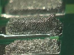
Solder paste is a mixture of solder alloy particles and flux, used to create electrical and mechanical connections between SMD components and the PCB.
Key Properties of Solder Paste
- Viscosity for consistent printing
- Metal content for strong solder joints
- Flux activity for proper wetting and oxidation removal
Selecting the right solder paste is essential for stable SMT manufacturing, especially in double-sided PCB assembly.
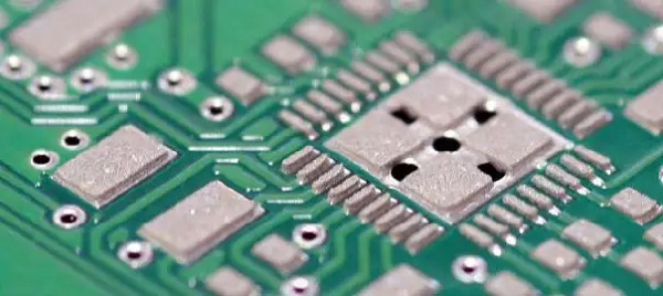
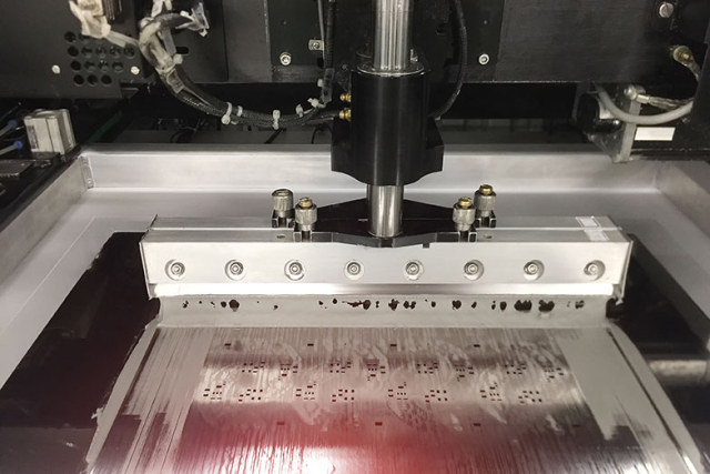
Stencil Design for Double-Sided PCBs
The stencil plays a critical role in controlling the volume and placement of solder paste.
1. Stencil Thickness Optimization
Proper stencil thickness ensures accurate solder volume:
- Thicker stencil → more solder paste (for larger components)
- Thinner stencil → finer control (for fine-pitch components)
For double-sided PCBs, balancing stencil thickness is crucial for both sides.
2. Aperture Design and Reduction
Stencil aperture design directly impacts solder paste deposition.
- Use aperture reduction for fine-pitch components
- Optimize shape (rectangular, rounded) to improve release
- Prevent solder bridging and insufficient solder
3. Step Stencil Technology
For complex double-sided PCB designs, step stencils allow:
- Different thickness regions on the same stencil
- Accurate solder volume control for mixed component sizes
Key Considerations for Double-Sided PCB Assembly
1. First-Side vs Second-Side Printing Strategy
In double-sided SMT assembly, the sequence matters:
- First side: usually smaller or lighter components
- Second side: components must withstand reflow heat without falling
Proper process planning ensures assembly stability.
2. Solder Paste Selection for Double Reflow
The solder paste must support:
- Multiple reflow cycles
- Strong initial tackiness to hold components
- Stable performance without degradation
3. Component Retention During Second Reflow
During the second reflow process:
- Components on the first side must remain attached
- Use appropriate solder paste volume and reflow profile
- Consider adhesive or optimized placement for heavier components
4. Reflow Profile Optimization
A well-controlled reflow soldering profile is critical:
- Avoid excessive temperature gradients
- Ensure proper solder melting and solidification
- Minimize thermal stress on components
Common Defects and How to Prevent Them
1. Solder Bridging
Cause: Excess solder paste or poor stencil design
Solution: Optimize aperture size and stencil thickness
2. Insufficient Solder
Cause: Inadequate paste deposition
Solution: Adjust stencil opening and printing parameters
3. Tombstoning
Cause: Uneven heating or imbalance in solder wetting
Solution: Improve thermal profile and pad design
4. Component Drop-Off (Second Side)
Cause: Weak solder joints during second reflow
Solution: Use high-quality solder paste and optimized process control
Best Practices for Solder Paste Printing and Stencil Design
To achieve high-quality double-sided PCB assembly, follow these best practices:
- Use high-quality solder paste with stable performance
- Optimize stencil thickness and aperture design
- Apply step stencil for mixed component layouts
- Control printing parameters (pressure, speed, alignment)
- Validate with SPI (Solder Paste Inspection) and AOI
- Work with experienced PCB assembly manufacturers
Applications of Double-Sided PCB Assembly
Double-sided PCBs are widely used in:
- Consumer electronics
- Telecommunication devices
- Automotive electronics
- Industrial control systems
These applications benefit from high-density and efficient SMT assembly.
Conclusion
Proper management of solder paste and stencil design is essential for successful double-sided PCB assembly. By optimizing printing parameters, selecting the right materials, and controlling the reflow process, manufacturers can significantly improve solder joint reliability and reduce defects.
In high-density SMT PCB manufacturing, attention to these details ensures consistent quality and long-term performance.
