
As electronic products continue to evolve toward higher density, faster signal transmission, and greater reliability, traditional through-hole processing is no longer sufficient for many advanced PCB designs. Technologies such as HDI (High-Density Interconnect), BGA (Ball Grid Array), and fine-pitch surface-mount devices often require plated through holes with improved mechanical strength and completely sealed surfaces.
PCB plating hole filling technology, also known as electroplated via filling, is a specialized manufacturing process that fills plated through holes or vias with copper during electroplating. Unlike conventional through-hole plating, which deposits copper only on the hole wall, plating hole filling gradually deposits copper until the hole is completely or nearly completely filled.
This technology improves PCB reliability, supports via-in-pad designs, enhances thermal performance, and enables higher routing density for advanced electronic products.
1. What Is PCB Plating Hole Filling Technology?
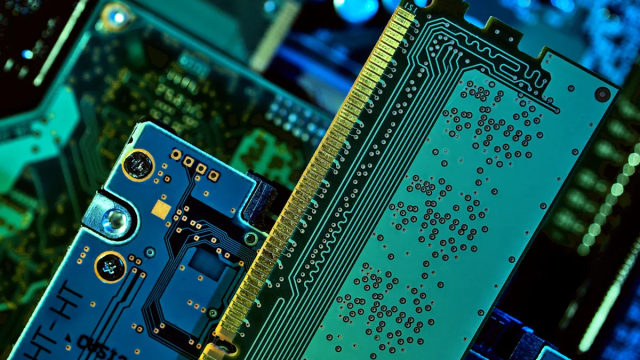
PCB plating hole filling is an electroplating process in which copper is deposited inside a drilled via until the hole is substantially or completely filled with solid copper.
Compared with conventional through-hole plating:
- Standard Through-Hole Plating
- Copper coats only the inner wall of the hole.
- The center of the hole remains hollow.
- Plating Hole Filling
- Copper continues depositing inside the hole.
- The via becomes completely or nearly completely filled.
This process is commonly used for:
- Blind vias
- Microvias
- Via-in-pad structures
- High-density multilayer PCBs
2. Why Is Hole Filling Needed?
As PCB component density increases, designers face several challenges:
- Limited routing space
- Reduced pad size
- Higher current density
- Faster signal transmission
- Improved thermal dissipation requirements
Traditional hollow vias may create issues such as:
- Solder wicking during SMT assembly
- Reduced solder joint reliability
- Uneven pad surfaces
- Mechanical weakness
- Thermal limitations
Copper-filled vias help overcome these problems while enabling more compact PCB layouts.
3. PCB Plating Hole Filling Process
A simplified process flow is shown below:
Drilling
↓
Desmear & Hole Cleaning
↓
Electroless Copper Deposition
↓
Pattern Electroplating
↓
Copper Via Filling
↓
Surface Planarization
↓
Surface Finish
↓
Inspection & Testing
4. Key Process Steps
4.1 Drilling
Mechanical or laser drilling creates the required vias.
Common hole types include:
- Through holes
- Blind vias
- Buried vias
- Laser microvias
Hole quality directly affects filling performance.
4.2 Hole Preparation
Before plating, the hole is cleaned to remove:
- Resin residue
- Debris
- Oxidation
Typical processes include:
- Desmear
- Chemical cleaning
- Surface activation
Proper preparation improves copper adhesion.
4.3 Electroless Copper Deposition
A thin conductive copper layer is chemically deposited on:
- Hole walls
- PCB copper surfaces
This seed layer allows subsequent electroplating.
4.4 Electroplated Copper Filling
This is the core of the process.
Using specially formulated plating chemistry and carefully controlled current density, copper deposits preferentially inside the via until it is filled.
Critical process parameters include:
- Current density
- Copper ion concentration
- Organic additives
- Bath temperature
- Agitation and solution flow
Process stability is essential to avoid defects.
4.5 Surface Planarization
After filling, excess copper is removed to create a flat surface.
Methods include:
- Mechanical polishing
- Grinding
- Chemical Mechanical Planarization (CMP)
A smooth surface is particularly important for via-in-pad designs.
5. Types of Hole Filling
5.1 Complete Copper Filling
The via is entirely filled with solid copper.
Advantages:
- Excellent thermal conductivity
- High mechanical strength
- Ideal for via-in-pad
Applications:
- HDI PCBs
- High-speed digital boards
- Semiconductor test boards
5.2 Partial Copper Filling
Only part of the via is filled.
Advantages:
- Lower manufacturing cost
- Suitable for applications that do not require complete filling
5.3 Copper Filling with Resin Plugging
The via is first filled with resin, then copper plated over the surface.
Advantages:
- Flat pad surface
- Excellent SMT performance
- Good mechanical reliability
Applications:
- BGA packages
- Fine-pitch SMT components
6. Advantages of PCB Plating Hole Filling
6.1 Supports Via-in-Pad Design
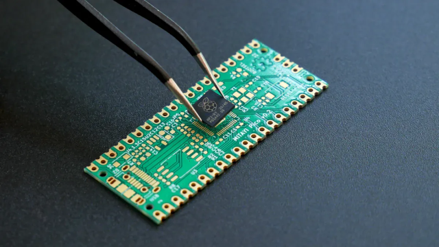
Via-in-pad technology places vias directly inside component pads.
Copper-filled vias prevent:
- Solder loss into the via
- Voids under solder joints
- Assembly defects
This improves SMT reliability.
6.2 Improves Thermal Management
Solid copper provides a highly efficient thermal path.
Heat can transfer from:
- Power devices
- CPUs
- LEDs
- RF power amplifiers
to internal copper planes more effectively.
Applications include:
- Power electronics
- Automotive electronics
- LED lighting
6.3 Enhances Mechanical Reliability
Copper-filled vias offer:
- Increased structural strength
- Better resistance to thermal cycling
- Reduced risk of via cracking
6.4 Enables Higher Routing Density
Filled vias allow:
- Smaller pads
- Tighter routing
- Higher component density
This is essential for:
- HDI PCB
- Smartphone PCBs
- AI accelerator boards
6.5 Improves Electrical Performance
Compared with hollow vias, copper-filled vias can provide:
- Lower electrical resistance
- More consistent current paths
- Reduced impedance variation
These characteristics support high-speed signal transmission.
7. Manufacturing Challenges
7.1 Void Formation
If plating parameters are not optimized, voids may remain inside the via.
Potential consequences:
- Reduced thermal conductivity
- Lower mechanical strength
- Reliability concerns
7.2 Surface Unevenness
Overfilling or underfilling may result in:
- Uneven pad surfaces
- Poor solder joint quality
Accurate planarization is required.
7.3 Process Control Complexity
Hole filling requires precise control of:
- Plating chemistry
- Current distribution
- Temperature
- Bath maintenance
Compared with standard electroplating, the process is significantly more demanding.
8. Typical Applications
HDI PCBs
Applications:
- Smartphones
- Tablets
- Wearable devices
Semiconductor Test Boards
Applications:
- Load boards
- Probe cards
- High-speed test interfaces
Requirements:
- High reliability
- Excellent signal integrity
High-Speed Communication Equipment
Applications:
- Network switches
- Data center hardware
- 5G infrastructure
Advantages:
- Higher routing density
- Improved electrical performance
Automotive Electronics
Applications:
- ADAS systems
- Powertrain controllers
- Battery management systems (BMS)
Requirements:
- High reliability
- Thermal stability
Power Electronics
Applications:
- Motor drives
- Inverters
- DC-DC converters
Advantages:
- Improved heat dissipation
- Higher current capability
9. Inspection and Quality Control
Copper-filled vias typically undergo:
X-ray Inspection
Verifies:
- Void-free filling
- Internal copper structure
Cross-Section Analysis
Confirms:
- Filling quality
- Copper thickness
- Hole integrity
Thermal Cycling Tests
Evaluates long-term reliability under repeated temperature changes.
Electrical Testing
Checks:
- Continuity
- Resistance
- Insulation performance
10. Design Considerations
When designing PCBs that require plated hole filling, engineers should consider:
- Via diameter
- Aspect ratio
- Copper thickness
- Stack-up design
- Thermal requirements
- SMT component placement
- Manufacturing capability
Early Design for Manufacturability (DFM) analysis helps ensure the selected via structure can be produced consistently while controlling cost and improving yield.
Conclusion
PCB plating hole filling technology has become a key manufacturing process for advanced electronic products that require high-density routing, improved thermal performance, and enhanced reliability.
Compared with conventional plated through holes, copper-filled vias offer significant advantages in:
- SMT assembly quality
- Mechanical strength
- Heat dissipation
- Electrical performance
- PCB miniaturization
As technologies such as HDI PCBs, AI computing, automotive electronics, 5G communications, and power electronics continue to evolve, plating hole filling will remain an essential process for enabling compact, high-performance, and highly reliable PCB designs.
