
As electronic devices become smaller, smarter, and increasingly battery-powered, reducing power consumption has become a key objective in PCB design. Whether developing IoT sensors, wearable devices, medical electronics, or industrial control systems, an optimized low power PCB extends battery life, reduces thermal stress, and improves overall system reliability.
Low power PCB design is far more than selecting low-power components. It requires a comprehensive approach that considers circuit architecture, PCB layout, power distribution, signal integrity, and system-level power management throughout the entire design process.
Understanding Power Consumption in PCB Design
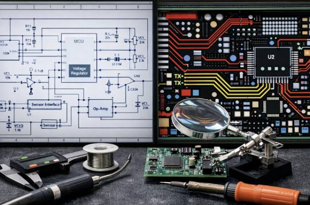
Power consumption in electronic circuits generally consists of two components:
Dynamic Power
Dynamic power is consumed when circuits switch states. It is primarily affected by:
- Switching frequency
- Supply voltage
- Capacitive loading
- Signal transition time
- Switching activity
As operating frequency increases, dynamic power often becomes the dominant contributor to total power consumption.
Static Power
Static power is consumed even when a circuit is idle, mainly due to leakage currents within semiconductor devices. As process geometries continue to shrink, leakage current has become an increasingly important consideration for low-power electronics.
Reducing both dynamic and static power is essential for achieving an energy-efficient PCB design.
Key Strategies for Low Power PCB Design
Select Low-Power Components
Component selection forms the foundation of every low power design.
When evaluating processors, MCUs, FPGAs, PMICs, and analog devices, engineers should consider:
- Low operating current
- Low standby current
- Minimal leakage current
- High conversion efficiency
- Built-in sleep or deep power-down modes
Many modern MCUs provide multiple low-power operating modes that significantly reduce energy consumption during idle periods while maintaining fast wake-up capability.
Identify Major Power Consumers
Before optimizing the PCB layout, identify which devices consume the most power.
Common high-power components include:
- Microcontrollers
- Wireless communication modules
- LEDs
- Displays
- RF transmitters
- Motor drivers
A simple power budget calculation helps prioritize optimization efforts where they provide the greatest benefit.
Optimize PCB Size and Layer Stackup
PCB geometry directly influences power efficiency.
A well-designed stackup helps reduce:
- Trace resistance
- Parasitic capacitance
- Voltage drop
- Switching noise
Typical recommendations include:
- Keeping power paths short
- Minimizing unnecessary vias
- Reducing loop area
- Placing power and ground planes adjacent to each other
Adjacent power and ground planes create additional interplane capacitance, lowering PDN impedance and improving power integrity.
Design a Stable Power Distribution Network (PDN)
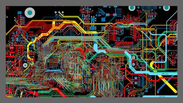
A low-impedance PDN ensures clean and efficient power delivery throughout the PCB.
Effective PDN design typically includes:
- Decoupling capacitors near IC power pins
- Bulk capacitors for transient current demands
- Ferrite beads for high-frequency noise suppression
- Proper power plane partitioning
- Continuous ground reference planes
Stable power distribution improves signal integrity while reducing unnecessary power loss.
Reduce Switching Frequency When Possible
Dynamic power is directly related to switching frequency.
When application requirements allow, reducing clock frequency or PWM switching frequency can significantly lower power consumption.
Variable-frequency control techniques and PWM duty-cycle optimization further improve system efficiency under changing load conditions.
Minimize EMI to Improve Efficiency
Electromagnetic interference increases switching noise and may indirectly increase power consumption.
Good EMI practices include:
- Separating switching regulators from sensitive analog or RF circuits
- Keeping high-current loops small
- Using proper grounding techniques
- Adding output filtering where necessary
- Maintaining continuous return paths
Reducing EMI also improves overall system stability.
Reduce Leakage Current
For ultra-low-power applications, leakage current becomes increasingly important.
Common design techniques include:
- Guard rings
- High-quality insulation materials
- Proper PCB surface cleanliness
- Ceramic standoffs for extremely low-current circuits
Although these techniques are generally reserved for nanoamp-level applications, they are essential in precision instrumentation.
Memory Power Optimization
Flash memory and external storage devices often consume unnecessary standby power.
Two common approaches include:
Power Switching
External MOSFETs controlled by an MCU can disconnect unused memory devices during standby operation.
Ultra-Deep Power Down (UDPD)
Many modern SPI Flash devices support UDPD mode, allowing the MCU to place the memory into an ultra-low-power state without additional external circuitry.
This approach reduces standby current while simplifying hardware design.
Advanced Power Management Techniques
Power Gating
Power gating disconnects unused circuit blocks from the power supply during idle operation.
Typical applications include:
- Wireless modules
- Sensors
- Displays
- Peripheral interfaces
By completely removing power from inactive circuits, standby consumption can be dramatically reduced.
Clock Gating
Clock gating disables clock signals to inactive logic blocks while keeping the rest of the system operational.
Benefits include:
- Lower dynamic power consumption
- Reduced switching activity
- Improved thermal performance
Clock gating is widely implemented in modern processors, SoCs, and FPGA designs.
Dynamic Voltage and Frequency Scaling (DVFS)
DVFS adjusts operating voltage and clock frequency according to processing demand.
During light workloads, the system operates at lower voltage and frequency to minimize energy consumption.
When combined with clock gating and power gating, DVFS provides one of the most effective strategies for maximizing battery life.
Typical Applications of Low Power PCB Design
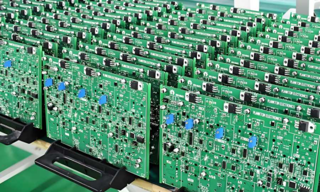
Low power PCB design is widely used in applications where energy efficiency and long operating life are essential, including:
- IoT devices
- Wireless sensors
- Wearable electronics
- Medical monitoring equipment
- Smart home products
- Industrial automation
- Portable test instruments
- Battery-powered consumer electronics
These systems benefit from reduced heat generation, longer battery life, and improved operational reliability.
Conclusion
Effective low power PCB design requires careful consideration of component selection, PCB layout, power distribution, stackup design, and advanced power management techniques. By minimizing dynamic and static power consumption while maintaining signal integrity and system stability, engineers can develop energy-efficient products that meet the growing demands of modern electronics.
At KKPCB, our engineering team supports customers throughout the entire development process—from PCB design review and stackup optimization to prototype fabrication and turnkey PCB assembly. Through Design for Manufacturability (DFM), controlled manufacturing processes, and advanced PCB technologies, we help accelerate product development while delivering reliable, high-quality PCB solutions for low-power electronic applications.
