
With the rapid development of industrial automation, IoT devices, smart manufacturing, medical electronics, and intelligent monitoring systems, sensors and transducers have become essential components in modern electronic products.
A sensor detects physical parameters from the surrounding environment, while a transducer converts these physical signals into electrical signals that can be processed by electronic circuits.
In PCB design, integrating sensors and transducers is not simply a matter of connecting components. Their performance is strongly influenced by:
- Signal integrity
- Noise control
- Power stability
- Analog circuit layout
- Thermal effects
- Mechanical placement
A well-designed sensor PCB must ensure that weak measurement signals are accurately captured and processed while avoiding interference from digital circuits, power components, and external environmental factors.
This article explains the role of sensors and transducers in PCB design, key design considerations, common challenges, and best practices for achieving reliable measurement performance.
1. Understanding Sensors and Transducers
1.1 What Is a Sensor?
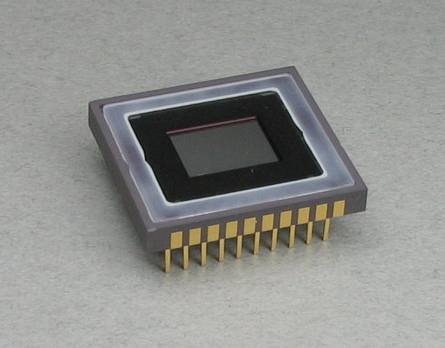
A sensor is an electronic component that detects changes in physical conditions and generates a corresponding electrical output.
Common measured parameters include:
- Temperature
- Pressure
- Humidity
- Light intensity
- Magnetic field
- Motion
- Acceleration
- Vibration
- Gas concentration
Examples include:
- Temperature sensors
- Hall-effect sensors
- Optical sensors
- Accelerometers
- Pressure sensors
1.2 What Is a Transducer?
A transducer converts one form of energy into another, typically converting physical energy into an electrical signal.
Examples:
| Physical Input | Transducer Output |
|---|---|
| Temperature | Voltage/resistance change |
| Pressure | Electrical signal |
| Sound | Electrical waveform |
| Mechanical movement | Electrical signal |
| Light | Current/voltage |
In many electronic systems, sensors are a type of transducer because they convert physical measurements into electrical information.
2. Role of Sensors and Transducers in PCB Systems
Sensors and transducers are usually integrated with supporting circuits on a PCB, including:
- Signal conditioning circuits
- Amplifiers
- Filters
- Analog-to-digital converters (ADC)
- Microcontrollers
- Communication interfaces
A typical sensor signal chain includes:
Physical Parameter
        ↓
Sensor / Transducer
        ↓
Signal Conditioning
        ↓
ADC Conversion
        ↓
MCU Processing
        ↓
Communication / Control Output
Each stage can affect measurement accuracy.
3. Key PCB Design Challenges for Sensor Applications
3.1 Signal Integrity of Low-Level Analog Signals
Challenge
Many sensors generate very small output signals.
Examples:
- Millivolt-level voltage signals
- Microamp-level current signals
- Low-frequency analog outputs
These signals are vulnerable to:
- Noise coupling
- Ground interference
- Crosstalk
Poor PCB design may cause:
- Measurement errors
- Signal drift
- Reduced sensitivity
PCB Design Recommendations
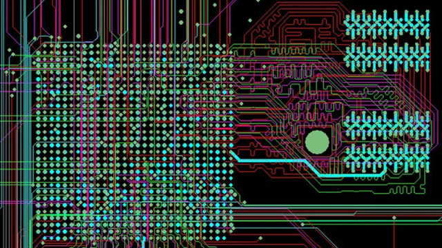
To improve signal integrity:
Keep Sensor Traces Short
Shorter traces reduce:
- Noise pickup
- Parasitic capacitance
- Signal attenuation
Separate Analog and Digital Areas
A recommended PCB structure:
Analog Sensor Area
        |
Signal Conditioning
        |
ADC
        |
Digital Processing Area
This prevents digital switching noise from affecting sensitive analog signals.
3.2 Power Supply Stability
Challenge
Many sensors require stable power supplies.
Voltage fluctuations may affect:
- Measurement accuracy
- Calibration stability
- Sensor response
Common sources of power noise:
- DC/DC converters
- Switching regulators
- Motors
- Relays
PCB Design Recommendations
Use:
- Local decoupling capacitors
- Low-noise voltage regulators
- Proper power filtering
For sensitive sensors:
- Avoid sharing noisy power rails.
- Consider dedicated LDO regulators.
3.3 Grounding Strategy
Challenge
Ground design is one of the most important factors in sensor PCB performance.
Incorrect grounding may introduce:
- Ground loops
- Voltage offsets
- Measurement instability
Recommended Grounding Approach
Separate:
- Analog ground (AGND)
- Digital ground (DGND)
Connect them at a controlled point near:
- ADC
- Signal processing interface
This reduces noise coupling between analog and digital sections.
3.4 Electromagnetic Interference (EMI) Control
Challenge
Industrial environments often contain strong interference sources:
- Motors
- Power converters
- Wireless modules
- High-current switching circuits
Sensitive sensor signals can be affected by:
- Electromagnetic radiation
- Conducted noise
- Switching transients
PCB Design Recommendations
Consider:
- Ground shielding
- Guard traces
- Filtering components
- Proper cable connections
For high-sensitivity applications:
- Add shielding structures.
- Keep sensors away from switching power sections.
3.5 Thermal Effects
Challenge
Temperature changes can affect:
- Sensor output
- Component characteristics
- Calibration accuracy
Examples:
- Resistance drift
- Offset changes
- ADC reference variation
PCB Design Recommendations
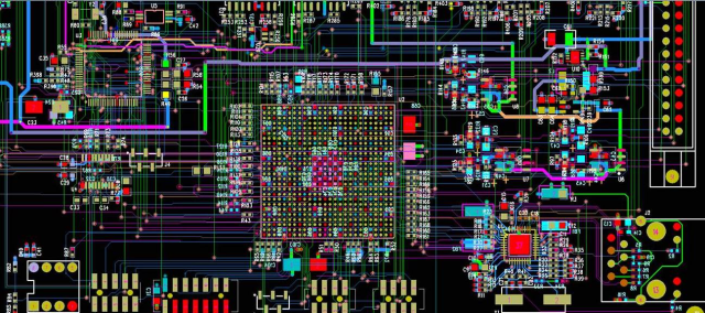
Consider:
- Heat source placement
- Thermal isolation
- Temperature compensation
Avoid placing sensitive sensors near:
- Power MOSFETs
- Regulators
- High-current components
4. PCB Layout Best Practices for Sensor Integration
4.1 Sensor Placement
Sensor location should consider:
- Measurement accuracy
- Environmental exposure
- Mechanical structure
Examples:
Temperature Sensor
Should be:
- Away from heat-generating components
- Close to the measurement target
Magnetic Sensor
Should avoid:
- Strong magnetic interference sources
- High-current traces
Pressure Sensor
May require:
- Mechanical openings
- Proper airflow paths
4.2 Analog Front-End Layout
The analog front end often includes:
- Operational amplifiers
- Filters
- ADC circuits
Layout recommendations:
- Keep components close together.
- Minimize signal loops.
- Avoid high-speed digital routing nearby.
4.3 Filtering Design
Sensor circuits commonly use:
- RC filters
- LC filters
- EMI suppression components
Filtering helps reduce:
- High-frequency noise
- Power supply disturbances
- External interference
4.4 ADC Layout Considerations
For ADC-based measurement systems:
Important factors include:
- Reference voltage stability
- Ground quality
- Input trace routing
Recommendations:
- Place ADC close to the analog section.
- Keep ADC inputs away from digital clocks.
5. Common Sensor PCB Applications
5.1 Industrial Automation
Applications:
- Pressure monitoring
- Temperature monitoring
- Current sensing
- Machine condition monitoring
Requirements:
- High reliability
- Long-term operation
- Noise resistance
5.2 Industrial IoT (IIoT)
Applications:
- Wireless sensor nodes
- Remote monitoring devices
- Smart equipment
Requirements:
- Low power consumption
- Reliable communication
5.3 Medical Electronics
Applications:
- Biosignal acquisition
- Patient monitoring devices
- Wearable sensors
Requirements:
- High signal accuracy
- Low noise design
5.4 Automotive Electronics
Applications:
- Position sensing
- Battery monitoring
- Environmental detection
Requirements:
- Temperature resistance
- Vibration reliability
6. Sensor PCB Manufacturing Considerations
6.1 PCB Material Selection
Common choices include:
FR-4 PCB
Suitable for:
- General sensor applications
- Industrial control boards
High-Tg PCB
Suitable for:
- High-temperature environments
- Industrial equipment
Flexible PCB
Suitable for:
- Wearable sensors
- Compact devices
6.2 Surface Finish Selection
Common finishes:
- ENIG
- ENEPIG
- HASL
For sensor boards requiring:
- High reliability
- Fine-pitch components
- Long service life
ENIG/ENEPIG may provide better consistency.
6.3 Assembly Requirements
Sensor PCBAs often require:
- High placement accuracy
- Fine-pitch SMT capability
- Reliable solder joints
Inspection methods include:
- SPI
- AOI
- X-ray inspection
- Functional testing
7. Improving Sensor PCB Reliability Through DFM Analysis
Early DFM review can identify potential risks such as:
- Difficult component placement
- Insufficient test points
- Signal interference issues
- Assembly limitations
A comprehensive review should consider:
Electrical Design
- Signal paths
- Power distribution
- Grounding
Mechanical Design
- Sensor location
- Mounting structure
- Environmental requirements
Manufacturing Design
- Assembly process
- Inspection accessibility
- Production consistency
8. Future Trends in Sensor PCB Design
8.1 Miniaturization
Future sensor PCBAs will require:
- Smaller form factors
- Higher integration
- HDI technology
8.2 Wireless Sensor Integration
More sensor systems will include:
- Bluetooth
- Wi-Fi
- LoRa
- Cellular communication
requiring improved RF PCB design.
8.3 Edge Computing Integration
Modern sensor boards increasingly combine:
- Sensors
- MCUs
- AI processing
- Communication modules
creating intelligent sensing platforms.
Conclusion
Sensors and transducers are fundamental building blocks in modern electronic systems, but their performance depends heavily on PCB design quality.
Reliable sensor PCB design requires careful consideration of:
- Signal integrity
- Power stability
- Grounding strategy
- EMI/EMC control
- Thermal management
- Manufacturing reliability
By optimizing sensor placement, analog layout, filtering, and production processes, engineers can achieve more accurate, stable, and durable measurement systems.
For industrial automation, IoT, medical devices, and intelligent equipment, a well-designed sensor PCBA provides the foundation for reliable data acquisition and smarter decision-making
