Mass flow meters are widely used in industrial automation, semiconductor manufacturing, chemical processing, medical gas systems, and energy monitoring applications. At the core of these systems is a highly reliable PCBA (Printed Circuit Board Assembly) that ensures accurate signal processing, stable sensor excitation, and precise flow measurement.
This case study presents a Mass Flow Meter PCBA solution, focusing on design architecture, sensor integration, signal conditioning, PCB layout strategy, and manufacturing reliability considerations for high-precision flow measurement systems.
Project Overview
The objective of this project was to develop a high-accuracy, low-drift PCBA solution for a next-generation mass flow meter system capable of:
- High precision gas flow measurement
- Long-term stability in industrial environments
- Low noise signal processing
- Multi-gas compatibility
- Compact PCB form factor
The system is designed for integration into thermal mass flow meters and Coriolis flow sensing platforms.
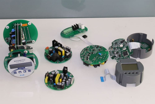
System Architecture of Mass Flow Meter PCBA
The PCBA solution is typically divided into several functional blocks:
1. Sensor Interface Section
- Thermal sensor or MEMS flow sensor input
- Wheatstone bridge configuration (for thermal sensing)
- High impedance analog front-end
2. Signal Conditioning Circuit
- Low-noise instrumentation amplifier
- Differential signal processing
- Filtering (low-pass / band-pass) for noise suppression
3. ADC Conversion Module
- High-resolution ADC (16-bit to 24-bit)
- Precision sampling for micro-flow detection
- Anti-aliasing filtering
4. Microcontroller / Processing Unit
- Real-time flow computation
- Temperature compensation algorithms
- Calibration curve storage
5. Communication Interface
- I²C / SPI for internal communication
- UART / RS485 / Modbus for industrial output
- Optional wireless integration
PCB Design Considerations for Mass Flow Meter PCBA
High-precision flow measurement requires extremely stable PCB design practices.
1. Low-Noise Analog Design
To ensure accurate signal acquisition:
- Separate analog and digital ground planes
- Use star grounding topology
- Minimize switching noise coupling
- Place ADC close to signal source
2. Sensor Signal Integrity
- Keep sensor traces short and symmetric
- Use guarded traces for high impedance nodes
- Avoid routing digital signals near analog front-end
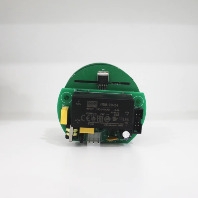
3. Power Supply Stability
- Use low-noise LDO regulators
- Add multi-stage decoupling capacitors
- Isolate analog and digital power rails
4. Thermal Stability Design
Thermal drift directly impacts flow accuracy:
- Place temperature sensors near flow sensor
- Use thermally balanced PCB layout
- Minimize heat sources near sensing area
5. EMI/EMC Control
Industrial environments introduce strong electromagnetic noise:
- Ground shielding around sensitive circuits
- Use RC filtering on input lines
- Implement EMI suppression capacitors
- Apply proper PCB layer stacking strategy
Material Selection for PCBA Reliability
For high-precision flow meter applications:
- FR4 high Tg material for stability
- Optional low-loss materials for high-frequency sensor systems
- ENIG surface finish for improved solder reliability
- Gold-plated contacts for long-term signal integrity
Manufacturing Process Highlights
The PCBA manufacturing process was optimized for high reliability and low defect rate:
1. SMT Assembly
- Precision placement for analog components
- AOI inspection after reflow
- Controlled reflow temperature profile
2. Through-Hole Components
- Reinforced solder joints for connectors
- Wave soldering for high-strength bonding
3. Testing and Calibration
- Functional flow simulation testing
- Zero-point calibration
- Multi-point flow accuracy validation
4. Aging Test
- Thermal cycling test
- Long-duration drift analysis
- Environmental stress screening
Key Engineering Challenges
1. Signal Drift
- Caused by temperature variation and component tolerance
- Solved using digital compensation algorithms
2. Noise Interference
- EMI from industrial motors and power lines
- Mitigated using shielding and PCB partitioning
3. Calibration Stability
- Required high-precision ADC and stable reference voltage
- Implemented precision voltage reference IC
Performance Results
After optimization, the PCBA solution achieved:
- High flow accuracy with low deviation
- Stable operation under wide temperature range
- Strong EMI resistance in industrial environments
- Improved long-term drift performance
- Compact and scalable PCB architecture
Applications
This Mass Flow Meter PCBA solution is widely applicable in:
- Semiconductor gas delivery systems
- Industrial automation control systems
- Medical ventilator and oxygen monitoring
- HVAC and environmental monitoring
- Chemical processing flow control
- Smart energy measurement systems
Conclusion
The Mass Flow Meter PCBA solution demonstrates how careful PCB design, low-noise analog engineering, and robust manufacturing processes can significantly improve measurement accuracy and system reliability.
By combining precision signal conditioning, thermal stability control, and EMI-resistant PCB architecture, modern flow meter systems can achieve high performance even in harsh industrial environments.
