
A Satellite PCB connector retention problem rarely begins with a broken connector. It begins when the board datum, cable load, shield bond, and support hardware are owned by different drawings. A connector can pass continuity at room temperature and still lose contact force, shift a coax launch, or load a solder joint during launch vibration and thermal cycling. This article presents a practical mechanical-electrical release method for project engineers who need repeatable connector retention without sacrificing the RF return path.
Where connector retention turns into an electrical failure
Satellite PCB connector retention becomes a system issue when a board edge is treated as a passive interface. A high-speed or RF connector carries signal current, return current, mechanical load, and often the only defined path between the cable shield and the chassis. If a bracket clamps the board from an offset datum, the connector can rotate slightly, the pin field can see uneven force, and the return path can develop a discontinuity that is invisible in a simple continuity check.
Begin with the failure chain rather than the connector part number. List the cable mass, bend radius, harness tie points, connector mating cycles, fastener locations, board thickness, stiffener edges, and the expected vibration axes. A PCB layout review should put these mechanical loads beside the signal pairs, launch pads, ground tabs, and keep-outs. The goal is to reserve copper and support points before the routing is closed.
For a project manager, the key decision is whether the connector is a replaceable service interface or a flight-retained interface. The former needs access and rework clearance; the latter needs controlled torque, locking hardware, and evidence that the load bypasses the soldered interface. A PCB prototype should reproduce the same support geometry if it is being used to validate retention.
Create one board-edge datum
A Satellite PCB connector retention drawing should name one board-edge datum and use it for connector centerline, mounting holes, standoffs, shield walls, stiffeners, and coax launches. Do not dimension the connector from a local copper feature while the bracket is dimensioned from the enclosure. That split creates an assembly tolerance stack that only appears when the parts are mated.
Define the datum in the fabrication drawing, assembly drawing, 3D mechanical model, and inspection program. Record finished board thickness, edge plating, hole position tolerance, connector seating surface, and the clearance to tall components. The multilayer PCB stack-up should state which layers support the connector pads and which layers carry the chassis return. If the connector crosses a material transition, identify that transition and the local drill-registration requirement.
For RF or controlled-impedance interfaces, the datum also controls the electrical length. A high-frequency PCB launch can be shifted by a small change in edge position, anti-pad clearance, or connector seating. Release a cross-section that shows the connector pin, pad, ground tabs, nearby vias, reference plane, and enclosure wall in one view. This is more useful than a generic connector footprint copied into several projects.
Size support and strain relief around the real load path
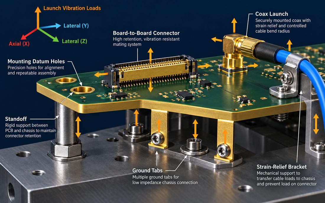
The connector should not be the only element resisting a harness load. Place support standoffs near the connector body and route cable force into the chassis through a bracket or tie point. A rigid support under one corner can create a lever arm that flexes the board at the opposite connector; a support too close to a plated edge can create local stress that changes the solder fillet or cracks the edge plating.
Map axial, lateral, and torsional loads separately. The rigid-flex PCB option can reduce cable bending at a board edge, but the stiffener termination, bend radius, adhesive, and connector strain relief must be dimensioned from the same datum. Do not let a flex tail transfer its bend moment directly into a high-density connector pad field.
Fasteners need a controlled interface definition. State washer type, torque window, locking method, contact surface, and whether the fastener is electrical ground or mechanical restraint. If a standoff carries heat, show the thermal path; if it only carries load, keep sensitive traces and vias clear. A DfMA review should also check tool access, connector mating clearance, depanelization edge, and the order in which the board, bracket, shield, and cable are installed.
Connector retention becomes harder when a component change moves a tall package into the support zone. Use component sourcing review to compare package height, keep-out, pin escape, and mechanical datum before an alternate connector or converter is released.
Protect shield and return continuity
Mechanical support cannot be separated from electromagnetic containment. Ground tabs, mounting screws, chassis fingers, via fences, and shield cans must connect without forcing return current through a narrow neck. A RF PCB launch should keep the first return vias close to the signal transition while preserving drill and assembly clearance. If the connector uses a metal shell, specify how that shell bonds to the board ground and the chassis.
Inspect the anti-pad and the ground-via field after the connector, bracket, and fastener positions are final. A late-added mounting hole can cut the return fence; a bracket coating can isolate a shield tab; an oversized washer can short a keep-out. Use a PCB materials review to confirm surface finish, edge plating, dielectric thickness, and any coating or mask boundary that affects the contact.
For differential pairs, maintain the reference plane through the connector escape and keep pair spacing consistent through the first transition. For power and low-speed harnesses, separate noisy returns from sensitive sensor returns before they reach the connector shell. The correct choice depends on the system architecture, but the decision must be visible in the controlled stack-up and interface notes.
Release assembly and inspection evidence
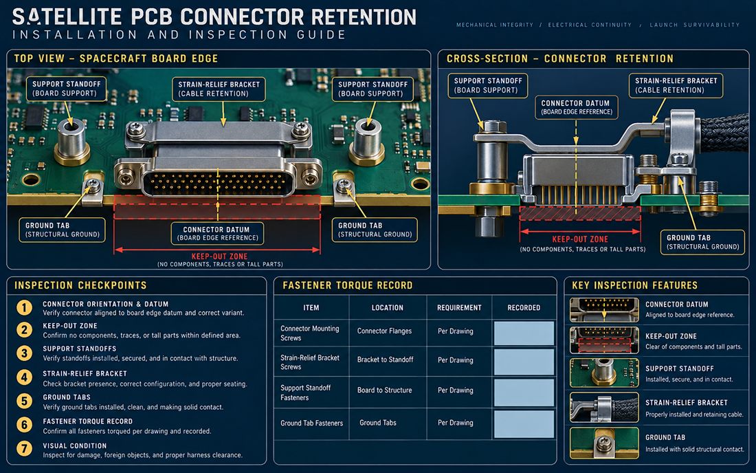
Assembly release should specify connector orientation, seating sequence, solder profile, cleaning process, bake or storage conditions, shield installation, and the inspection points that prove the board was not loaded during mating. PCB assembly records should link connector lot, board revision, stencil or selective-solder condition, and visual acceptance criteria.
Use a fixture that references the same board-edge datum as the enclosure. Check connector coplanarity, pad wetting, shell-to-ground contact, standoff contact, bracket seating, and the clearance to adjacent components. A quality control traveler should include a torque record and a photo or dimensional record for each critical retention feature. These are design-verification records for the release vehicle, not claims of a customer measurement.
Where RF performance matters, use a representative coupon or release vehicle that keeps the connector, launch, return fence, and bracket geometry. A controlled-impedance PCB check should record the fixture, calibration, connector torque, and temperature condition. If a cable assembly is changed, repeat the check because cable shield termination and bend force can change the board interface.
Control changes before qualification
Before qualification, freeze the connector family, board edge, datum holes, standoff pattern, cable bend limit, shell bond, and inspection method in one release package. A PCB manufacturing handoff should include the edge-finish, drill, plating, copper-balance, and panelization controls that affect connector position.
Use aerospace PCB assembly controls for traceability when the board is part of a flight-like vehicle, and use PCB assembly capabilities review to verify that inspection and rework can be performed without changing the datum. Keep standard PCB capacity assumptions separate from the high-frequency process window so that a schedule change does not silently alter the connector build.
A Satellite PCB connector retention release is credible when a technician can assemble the board, a fabricator can hold the datum, an engineer can trace the return path, and a project manager can see which change would force a new verification vehicle. That shared evidence is what prevents a small bracket or cable change from becoming a late spacecraft integration failure.
Sources: connector manufacturer application data; NASA workmanship and vibration guidance; laminate manufacturer dimensional-stability data; Analog Devices thermal and mixed-signal layout notes; Qorvo RF packaging references; and Würth high-frequency interconnect guidance. Values are engineering targets or typical design inputs, not customer measurements.





