
Ka-band front ends often use grounded coplanar waveguide (GCPW) because the signal and return path can stay on one layer near a connector or active device. The challenge is holding the gap, via-fence geometry, solder-mask opening, and reference plane together after fabrication. This guide shows how an RO5880 PCB GCPW release can address those engineering risks without claiming unverified test results.
Why GCPW is attractive for a Ka-band module
GCPW keeps ground close to the RF trace and can simplify launch transitions in a compact module. It is also sensitive to the spacing between the center trace and coplanar grounds. On a high-frequency PCB, a small gap shift, mask web, or missing via can change impedance and return-current distribution. Treat the top view and cross-section as one design object.
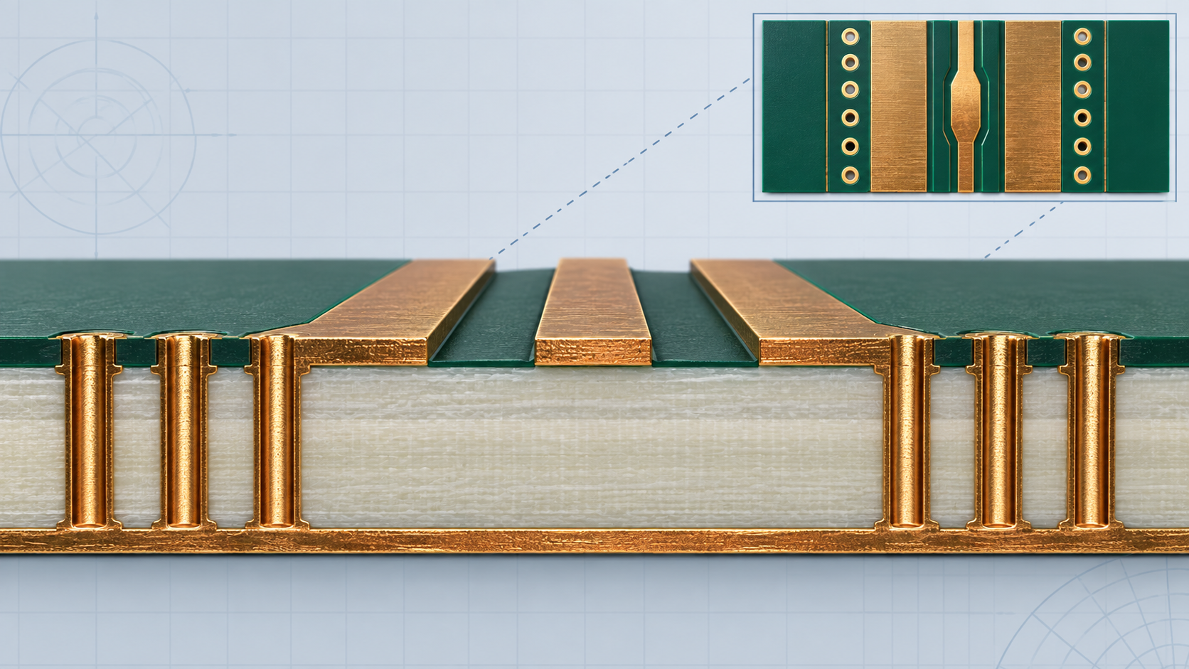
Set the electrical frame first
Define the finished trace width, gap, copper thickness, dielectric spacing, and reference-plane location. Rogers publishes typical RO5880 material values, but the design value must be correlated to the finished stackup. On a new RO5880 PCB, record the assumed mask condition and surface-finish route in the controlled-impedance table so a later DFM change does not quietly change the field geometry.
RO5880 PCB via fence as a return-current structure
An RO5880 PCB GCPW fence is part of the RF circuit, so its geometry must be released with the transition.
Via fences are not decorative stitching. They constrain the return path and reduce leakage around a bend, launch, or shield edge. Place the fence using the electrical model, then check drill, antipad, and registration rules with the fabricator. If the fence must pass through a mixed-material stackup, confirm that the plated barrel and reference planes remain continuous through every layer.
| GCPW feature | Common risk | Release control |
|---|---|---|
| Center trace-to-ground gap | Impedance shifts with etch or mask | State finished gap and mask keep-out |
| Via-fence pitch | Return path becomes discontinuous | Show fence rule and drill registration basis |
| Connector launch | Pad, ground, and housing do not share a datum | Review launch in top view and cross-section |
| Bend or taper | Current crowds at the corner | Use a controlled transition and inspect the copper edge |
Keep solder mask and copper fill out of the field
Solder mask can load a narrow GCPW gap, while copper fill can change the ground boundary or create an unintended resonant feature. Mark the RF keep-out on every copper and mask layer. For an impedance-controlled PCB, align the field-solver assumption with the fabrication drawing instead of relying on a generic mask default.
Plan the Ka-band launch and component handoff
A GCPW launch on an RO5880 PCB should transition through connector, package, or microstrip geometry without an abrupt return-path break. Keep the launch pad, ground vias, and enclosure or shield boundary tied to one mechanical datum. If an RF module assembly changes the component or connector, recheck the launch rather than treating the footprint as electrically interchangeable.
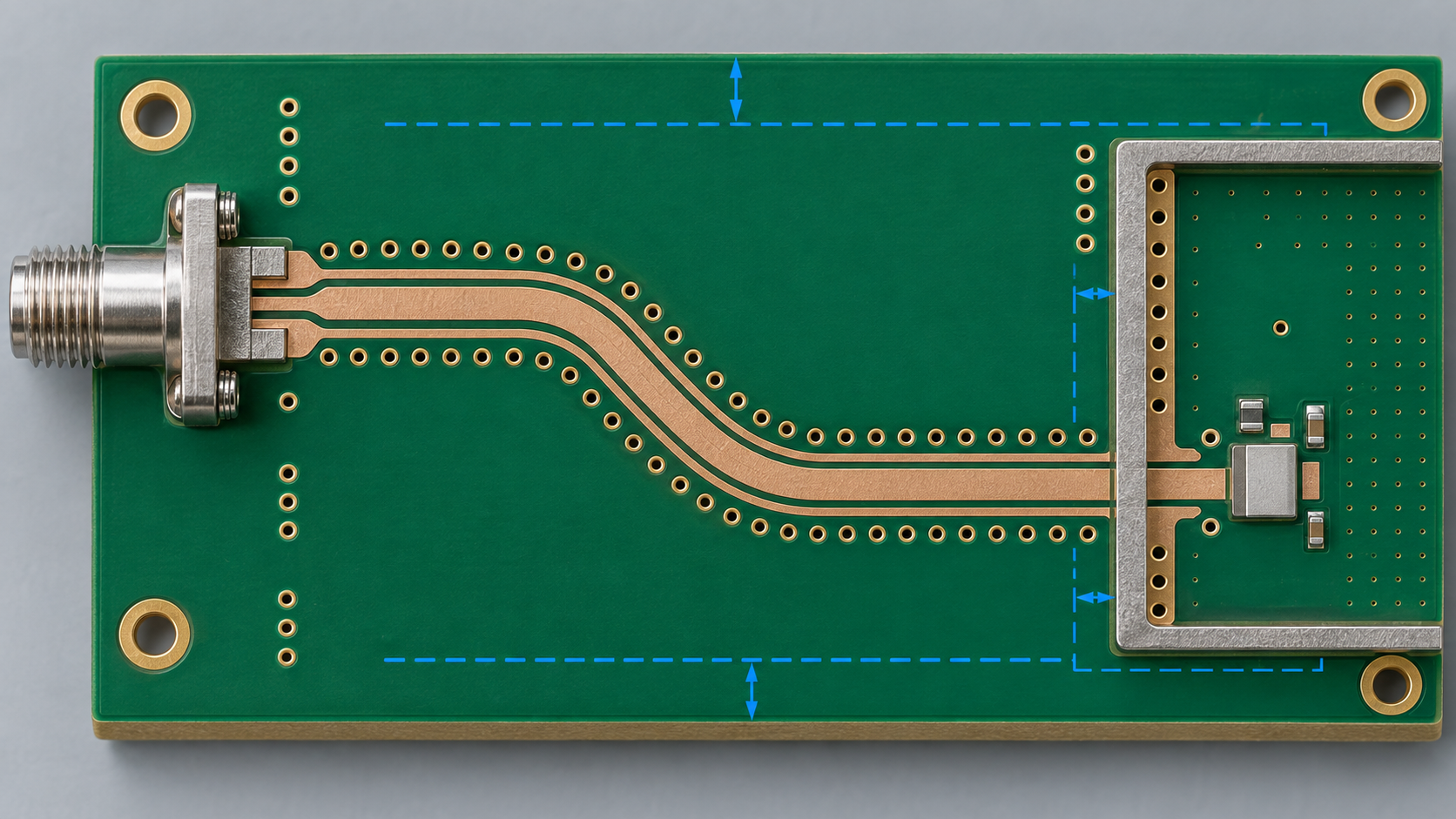
Use coupons that represent the GCPW geometry
An RO5880 PCB coupon should reproduce the same layer, trace-to-ground gap, copper, mask, via fence, and surface finish as the product route. A simple microstrip coupon cannot answer a GCPW question. Keep the coupon drawing with the stackup revision and identify which results are typical process values, targets, or measurements.
RO5880 PCB GCPW release checklist
- Define finished trace, gap, copper, mask, and reference-plane assumptions.
- Show via-fence pitch, drill, antipad, and registration controls.
- Review bends, tapers, connector launches, and enclosure boundaries.
- Keep copper fill and solder mask outside RF field regions.
- Use a GCPW coupon that matches the product layer pair and finish.
- Link layout, stackup, fabrication, and assembly revisions.
KKPCB can review an RO5880 PCB manufacturing release for GCPW geometry, via-fence registration, coupon coverage, and launch handoff. The review distinguishes laminate data, design targets, and measured evidence before tooling.
Key takeaway
A reliable RO5880 PCB GCPW route is a coordinated trace, gap, mask, via-fence, and reference-plane system. When those features are released together, Ka-band front-end teams can reduce launch surprises and debug the right variable. The same RO5880 PCB discipline scales to variants: preserve the electrical datum, recheck the coupon, and document every changed transition.
Sources: Rogers Corporation RT/duroid 5880 material information and fabrication guidance; IPC-TM-650 impedance, dimensional, and plating methods; KKPCB internal RF routing and manufacturing capability notes. Values are typical or target references unless explicitly identified as measured.
