
An RF design can pass simulation and still lose yield during assembly when solder-mask openings, land patterns, or shield clearances are not matched to the PCB stackup. This article explains how a controlled RO4003C PCB assembly package reduces those handoff risks for compact 5G and microwave modules.
Why assembly DFM matters for an RO4003C PCB
RF pads are part of the transmission path. A small mask web, an uneven solder joint, or a connector pad that is not coplanar can change the launch transition. At the same time, the laminate and copper must survive reflow without creating a mechanical shift. Treat the RF PCB assembly drawing as an extension of the RO4003C PCB stackup, not as a separate document written after layout.
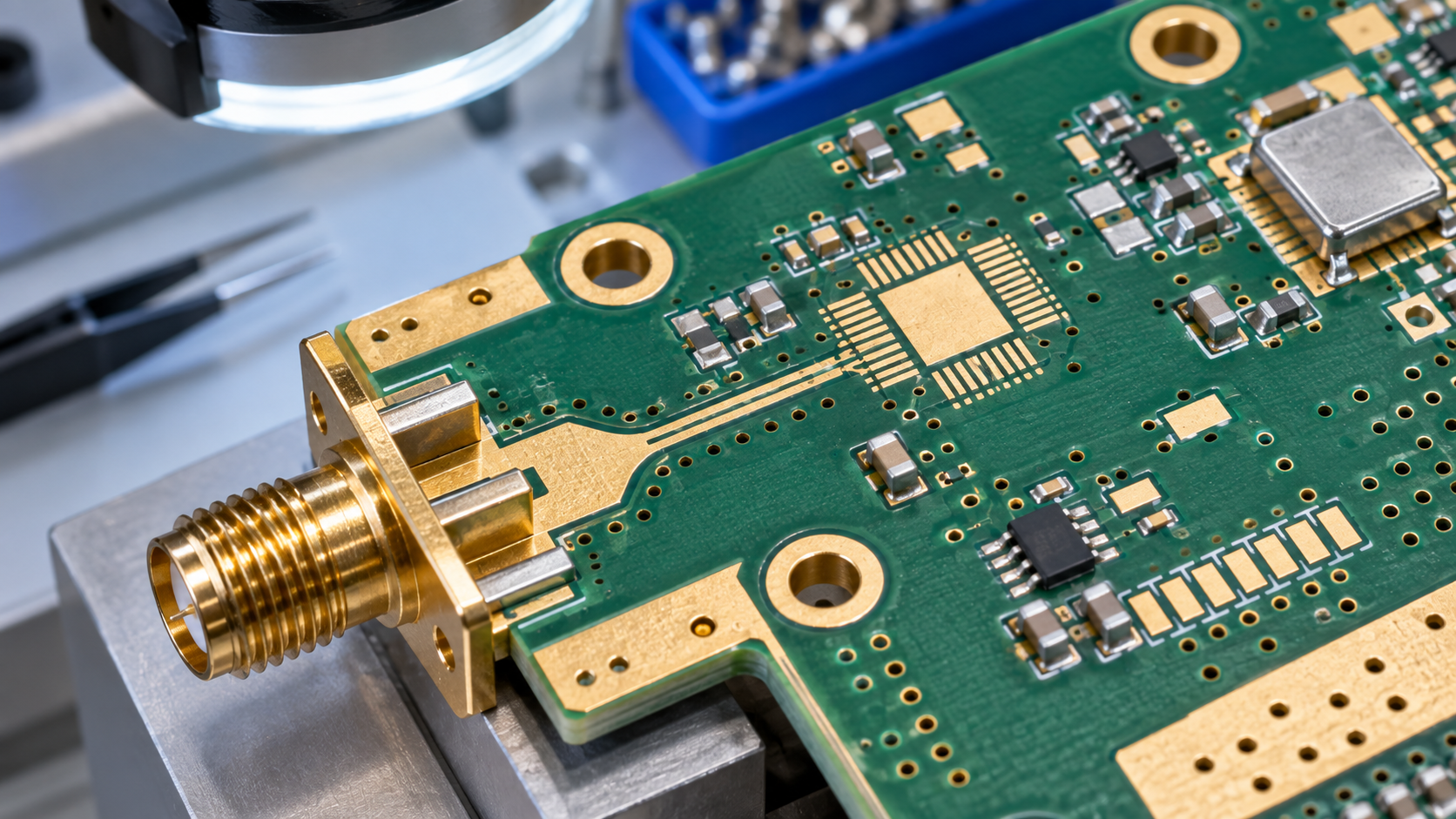
Lock the footprint to the RF transition
For each connector, amplifier, filter, or shielded module, define the pad geometry, mask expansion, via fence, and reference-plane clearance together. The RF designer should identify which pads are electrically active and which are mechanical. On a new RO4003C PCB layout, keep the connector datum and assembly datum visible so a pick-and-place rotation cannot silently mirror the feed.
RO4003C PCB land-pattern and solder-mask rules
For an RO4003C PCB, the land pattern and mask opening should be released as one RF feature.
Use the finished copper drawing to derive stencil apertures and mask openings. A larger aperture may improve solder volume but can also pull a fine RF pad during reflow. A mask web that is acceptable for a digital pad may bridge a sensitive feed or narrow a gap that the impedance model assumed to be open. Capture these choices in the assembly drawing and the fabrication drawing as one approved revision.
| Assembly feature | RF or yield risk | DFM control |
|---|---|---|
| RF launch pads | Uneven solder changes transition geometry | Use a defined pad, mask, and coplanarity review |
| Ground-via field | Voids or blocked vias disturb return current | Check drill, paste, and keep-out interaction |
| Shield land | Warp or paste imbalance affects seating | Balance aperture strategy and verify stencil support |
| Fine-pitch RF IC | Bridging or insufficient wetting | Align pad, paste, and inspection limits |
Coordinate stencil design with the RF keep-out
Stencil apertures should not be copied from a generic package library when the pad sits beside an antenna feed or a controlled-impedance line. The paste pattern, mask clearance, and copper pour need one review. If a PCB manufacturing change alters finished copper or mask registration, update the assembly drawing before the next build rather than treating it as an assembly-only issue.
Control reflow and mechanical stress
RO4003C PCB assemblies should use an approved reflow profile for the component package, finish, and board thickness. The project team should record the profile revision and any constraints on preheat, peak, or cooling. Avoid claiming a universal profile: the correct window depends on the component set and the assembler’s qualified process. Mechanical fixtures should support thin areas near connectors and keep the board flat through the heating cycle.

Use inspection to protect the RF intent
Visual inspection of an RO4003C PCB confirms mask, component orientation, and obvious bridging. X-ray or cross-section work can reveal voiding or hidden solder behavior beneath a shield or connector. Define the acceptance method before assembly begins, and identify whether a value is a target, a typical process limit, or a measured result. This keeps an impedance-controlled PCB discussion grounded in evidence.
Assembly handoff checklist
- Release one controlled footprint revision for each RF component and connector.
- Show mask openings, stencil apertures, ground-via fields, and RF keep-outs.
- Confirm board thickness, finish, and allowable support points for reflow.
- Document the qualified reflow profile and inspection method.
- Identify the RF transition features that require microscope, X-ray, or cross-section review.
- Keep fabrication, assembly, and test revisions linked by panel and lot traceability.
KKPCB can review an RF module assembly package for footprint clarity, mask coordination, and manufacturing handoff. The review distinguishes laminate data, design targets, and measured evidence so teams can close the highest-risk decisions first.
Key takeaway
A dependable RO4003C PCB is not finished when copper fabrication ends. The RO4003C PCB assembly land pattern, mask opening, paste strategy, and reflow support all influence the RF launch that the designer approved. By releasing those details together, teams can improve first-pass assembly yield without hiding uncertainty behind generic package rules.
Sources: Rogers Corporation RO4000 series laminate data sheet and RO4003C product information; IPC-TM-650 and IPC-A-610 assembly and inspection methods; KKPCB internal RF assembly and DFM capability notes. Any process limits are to be confirmed for the approved build and are not customer measured results.
