
Compact RF modules often fail between schematic approval and fabrication release because the RO4003C PCB stackup is treated as a static drawing. Resin content, copper thickness, press-out, and reference-plane choices change the field geometry that the RF model used. A controlled RO4003C PCB stackup release turns those assumptions into a buildable document for engineering and manufacturing.
Why stackup ownership matters in a compact RF module
A short feed can be more sensitive to dielectric thickness than to its nominal length. If a core or bondply moves during lamination, the finished trace-to-plane spacing changes and so does impedance. For a high-frequency PCB, the electrical model, material callout, and fabrication notes should be reviewed as one package. This is especially important when RF layers share a panel with digital circuitry or power copper.
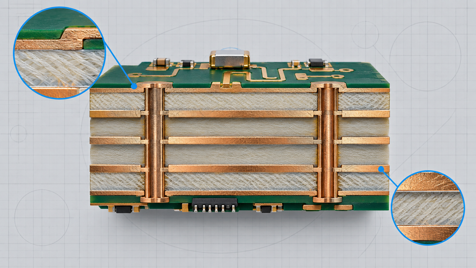
Separate material data from finished-board assumptions
Rogers publishes typical RO4003C laminate properties, including process and design dielectric-constant references. Those figures help start a model, but the finished board also depends on selected thickness, resin content, copper roughness, and the press cycle. A new RO4003C PCB release should label each value as a typical material value, a design target, or a measured result. If no measured result exists, leave the field open rather than implying one.
RO4003C PCB stackup choices manufacturing can hold
A production-ready RO4003C PCB stackup states the finished dielectric region, not only a catalog thickness.
Begin with the RF layer pair and its reference plane, then add digital and power layers around that electrical core. Keep the RF dielectric region as symmetric as the mechanical design allows. If asymmetry is required, note which side carries the larger copper image and what inspection evidence will confirm the final spacing.
| Stackup item | Project risk | Release action |
|---|---|---|
| RF dielectric thickness | Impedance and phase move with spacing | State the finished target and tolerance basis |
| Resin content | Press-out changes local geometry | Use the approved material construction and press note |
| Copper roughness | Loss and etch edge can vary | Call out foil type and finish route |
| Reference-plane continuity | Return current detours around voids | Review plane splits and via stitching before release |
Control RF and digital transitions
When a compact module combines RF and digital layers, keep high-speed transitions away from plane voids and large antipads. An RO4003C PCB RF stackup review should include via barrels, back-drill decisions, and the length of any unused stub. The objective is not the thinnest board; it is a repeatable field geometry that a fabricator can inspect and a test team can correlate.
Use a cross-section coupon to verify the build
A cross-section coupon for an RO4003C PCB should represent the RF layer pair, copper weight, and nearby plane pattern. Measure the finished dielectric region at several positions when the panel is large or copper density is uneven. Keep the coupon drawing with the stackup revision so a later variant cannot silently change the witness geometry.
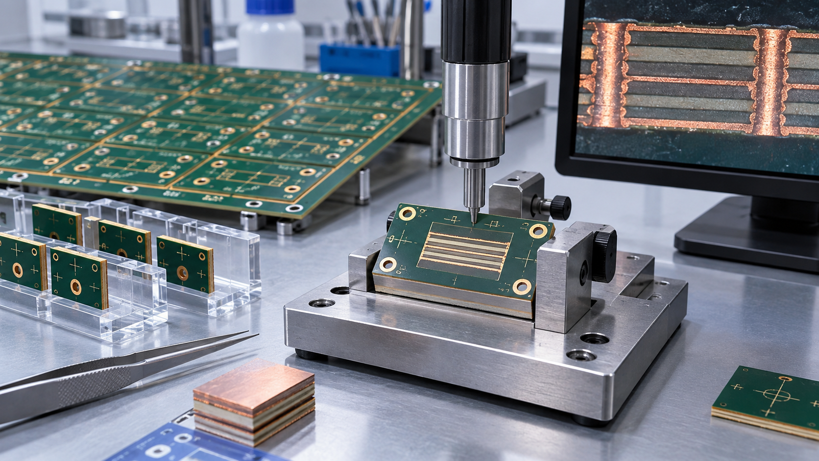
Define what the coupon does not prove
A coupon can confirm layer order, dielectric thickness, copper build, and registration at its location. It does not prove that every antenna feed has the same electromagnetic environment, nor does it replace product-level verification. Document that boundary in the inspection plan. For a controlled impedance PCB, pair coupon evidence with a traceability record that identifies panel, lot, stackup revision, and finish.
DFM checklist for an RO4003C PCB stackup
- Identify RF layers, reference planes, and any plane voids.
- State finished dielectric targets separately from nominal material thickness.
- Record copper foil, roughness assumption, and surface-finish route.
- Show via, antipad, back-drill, and return-path rules.
- Define representative cross-section and impedance coupons.
- Link the approved stackup to the panel drawing and inspection record.
KKPCB can review an RO4003C PCB multilayer PCB stackup for RF layer symmetry, press constraints, and coupon coverage before fabrication release. The review separates target values, typical material references, and measured values so project managers know which risks remain open.
Key takeaway
A reliable RO4003C PCB stackup is a controlled interface between field simulation and the press cycle. When the RF layer pair, dielectric construction, copper assumptions, and cross-section witness are released together, a compact module is easier to build and debug. The same RO4003C PCB discipline applies to later variants: preserve the electrical datum, document the process window, and re-qualify any changed layer construction.
Sources: Rogers Corporation RO4000 series laminate data sheet and RO4003C product information; IPC-TM-650 cross-section, dimensional, and impedance test methods; KKPCB internal multilayer and RF DFM capability notes. Values are typical references or targets unless explicitly identified as measured.
