
Why Material Selection Matters in Millimeter-Wave PCB Design
Millimeter-wave technology was once considered too expensive or technically difficult for widespread commercial applications. Today, that has changed rapidly.
The expansion of 5G New Radio (5G NR), 77 GHz automotive radar, ADAS, high-speed wireless communication, RF modules, and advanced sensing systems has made millimeter-wave PCB technology increasingly common in commercial electronics.
Unlike conventional low-frequency boards, a millimeter-wave PCB must manage electromagnetic performance at very short wavelengths. The PCB may contain multiple functional layers supporting digital, analog, RF, microwave, and millimeter-wave signals within the same compact assembly.
This creates a fundamental engineering challenge:
How can different circuit functions be integrated into one multilayer PCB without compromising RF performance, signal integrity, reliability, or manufacturing efficiency?
The answer often involves using a hybrid multilayer PCB material system, rather than using one material for every layer.
A high-frequency PCB may combine low-loss RF laminates with more economical FR-4 materials for power distribution, control circuits, or other layers where ultra-low dielectric loss is not required.
Therefore, choosing the right millimeter-wave PCB materials requires engineers to evaluate electrical, mechanical, thermal, and manufacturing properties together.

What PCB Material Properties Should Engineers Evaluate?
The first parameters normally considered are the dielectric properties of the material.
Dielectric Constant (Dk)
Dk affects the propagation velocity of an RF signal and directly influences transmission-line impedance and wavelength.
At millimeter-wave frequencies, stable Dk becomes increasingly important because small variations in dielectric properties can affect:
- Characteristic impedance
- Phase response
- Signal delay
- Antenna performance
- Radar pulse timing
- RF matching
For this reason, engineers should consider not only the nominal Dk value but also Dk stability across frequency, temperature, and material construction.
Dissipation Factor (Df)
Df represents dielectric loss.
As frequency increases, dielectric loss can become a significant part of total insertion loss. A low-Df material is therefore particularly important for applications with demanding RF link budgets.
For 5G mmWave PCB, 77 GHz radar PCB, and high-frequency RF circuits, material selection should consider the complete loss budget rather than evaluating Df in isolation.
CTE and Dimensional Stability
Mechanical properties become increasingly important as PCB structures become thinner and more densely layered.
The coefficient of thermal expansion (CTE), particularly in the Z-axis, affects:
- Plated through-hole reliability
- Via reliability
- Layer registration
- Thermal cycling performance
- Multilayer dimensional stability
For high-layer-count PCB designs, mechanical stability can be just as important as electrical performance.
Moisture Absorption
Moisture can affect dielectric properties and mechanical reliability.
Low moisture absorption is particularly valuable for automotive radar PCB, aerospace PCB, outdoor 5G equipment, and other electronics exposed to changing environmental conditions.
Why Hybrid Multilayer PCB Construction Is Often Practical
A complex multilayer board may contain several types of circuits.
For example:
Power layers → FR-4 or cost-effective materials
High-speed digital layers → low-loss/high-speed materials
RF layers → low-Df RF laminate
Millimeter-wave layers → ultra-low-loss RF material
This approach allows engineers to optimize material cost without sacrificing performance where it matters most.
However, hybrid construction introduces another challenge: the different materials must be laminated and interconnected reliably.
The selection process should therefore evaluate not only individual laminates but also:
Laminate + Prepreg + Copper + Stackup + Via + Lamination Process
This is one of the most important principles in high-frequency multilayer PCB material selection.
Rogers RO3003 for Millimeter-Wave PCB Applications
Rogers RO3003 is a ceramic-filled PTFE laminate widely associated with high-frequency and millimeter-wave circuit applications.
Its typical Z-axis Dk at 10 GHz is approximately 3.00, with a Df of approximately 0.0010.
The material is available in thicknesses ranging from approximately 0.005 to 0.060 inch (0.13 to 1.52 mm), depending on the product configuration.
RO3003 has been widely used in 77 GHz single-layer radar circuits and offers useful dimensional and thermal characteristics for multilayer structures.
Its X-Y CTE is approximately 17 ppm/°C, close to copper, which helps improve dimensional stability.
Its Z-axis CTE is approximately 25 ppm/°C, supporting reliable plated through-hole structures when properly processed.
Moisture absorption is also very low, approximately 0.04%, making it suitable for demanding RF environments.
For engineers searching for the best PCB material for 77 GHz radar, RO3003 can be considered when its electrical, mechanical, thickness, and manufacturing characteristics match the application requirements.
RO3003G2 for Lower-Loss Millimeter-Wave Circuits
At very high frequencies, copper surface roughness becomes increasingly important.
The conductor loss of an RF transmission line is influenced not only by the dielectric material but also by the interaction between the electromagnetic field and the copper surface.
Rogers RO3003G2 builds on the RO3003 material platform with an optimized filler system and smoother copper configuration.
It maintains similar dielectric characteristics while providing smoother copper for reduced conductor loss in demanding high-frequency applications.
RO3003G2 also maintains favorable X-Y CTE characteristics, while its optimized material structure provides a Z-axis CTE of approximately 18 ppm/°C, which is closer to copper.
Available thicknesses include approximately 0.005 inch (0.13 mm) and 0.010 inch (0.25 mm).
For millimeter-wave PCB design, this combination of low dielectric loss, dimensional stability, and smoother copper can be valuable when insertion loss is a critical design parameter.
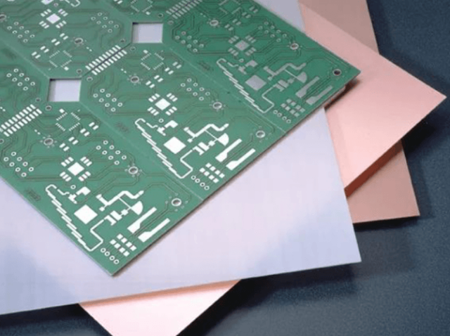
CLTE-MW for Thin and Dimensionally Stable Multilayer PCBs
When a design requires both low loss and reduced PCB thickness, CLTE-MW can be considered.
CLTE-MW uses a spread-glass structure and low-Dk ceramic filler system designed to provide high-frequency electrical performance and dimensional stability.
Its thickness range is approximately 0.003 to 0.010 inch (0.076 to 0.25 mm).
At 10 GHz, its typical Z-axis Dk is approximately 2.94 to 3.02, depending on thickness and construction.
The material also provides low moisture absorption of approximately 0.03% and favorable CTE characteristics for multilayer PCB fabrication.
This makes CLTE-MW relevant to applications where size, weight, signal loss, and mechanical stability must be optimized simultaneously.
Typical applications include:
- 77 GHz automotive radar
- ADAS radar modules
- 5G mmWave electronics
- RF front-end modules
- Compact wireless systems
- High-frequency instrumentation
Choosing the Right Prepreg and Bonding Material
A common mistake in multilayer RF PCB design is to focus only on the circuit laminate.
The bonding material is also part of the electrical structure.
Prepreg determines the final dielectric thickness between copper layers and contributes to the effective dielectric environment surrounding RF transmission lines.
Therefore, low-loss prepreg selection for multilayer PCB should consider:
- Dk
- Df
- Resin content
- Final dielectric thickness
- Glass-cloth construction
- Flow characteristics
- CTE
- Lamination compatibility
- Compatibility with PTFE or other RF laminates
Rogers 2929 Bonding Material
Rogers 2929 bonding material is designed for multilayer PCB construction and can support both standard and high-pressure bonding processes depending on the application.
Its typical Z-axis Dk at 10 GHz is approximately 2.94, while its Df is approximately 0.003.
Its electrical properties make it a candidate for multilayer structures using compatible PTFE-based RF laminates.
SpeedWave 300P
Rogers SpeedWave 300P is a low-loss prepreg designed for demanding multilayer RF applications.
Its typical Dk is approximately 3.0–3.3, depending on construction, while its Df is approximately 0.0019–0.0022 at 10 GHz.
It can be used with FR-4 and compatible PTFE-based circuit materials, including CLTE-MW.
Its low loss, flow characteristics, multiple glass-cloth configurations, and low Z-axis expansion make it attractive for high-layer-count RF PCB and millimeter-wave PCB applications.
Material Comparison for Millimeter-Wave PCB Design
| Material | Typical Dk @ 10 GHz | Typical Df @ 10 GHz | Main Advantage | Typical Application |
|---|---|---|---|---|
| RO3003 | 3.00 | 0.0010 | Low loss + dimensional stability | RF / 77 GHz radar |
| RO3003G2 | Similar to RO3003 | Similar to RO3003 | Smoother copper | Millimeter-wave RF |
| CLTE-MW | 2.94–3.02 | Very low loss | Thin + stable | 5G / radar / RF |
| Rogers 2929 | 2.94 | 0.003 | Low-loss bonding | Multilayer RF PCB |
| SpeedWave 300P | 3.0–3.3 | 0.0019–0.0022 | Low-loss prepreg | mmWave / high-layer PCB |
| FR-4 | Application dependent | Application dependent | Cost effectiveness | Power / control / digital |
Material data can vary by construction, frequency, thickness, glass style, and manufacturer test method. Final design values should always be verified against the applicable material datasheet.
DFM Considerations for High-Layer-Count Millimeter-Wave PCB
Material selection alone does not guarantee a reliable RF board.
A millimeter-wave PCB DFM review should be performed before production.
Control Finished Dielectric Thickness
The nominal prepreg thickness is not necessarily the final dielectric thickness after lamination.
Copper distribution, resin content, pressure, temperature, glass style, and adjacent structures can all affect the finished thickness.
Because dielectric thickness directly influences impedance, the stackup should be calculated using realistic finished dimensions.
Control Copper Roughness
At 77 GHz and other millimeter-wave frequencies, copper roughness can contribute significantly to conductor loss.
Engineers should specify suitable copper foil and surface roughness requirements for critical RF layers.
Minimize RF Via Discontinuities
RF vias can introduce parasitic inductance and capacitance.
Where possible, critical RF paths should minimize unnecessary layer transitions and optimize via diameter, pad size, anti-pad, via stub, and ground-via configuration.
Maintain Layer Registration
High-layer-count PCB structures require precise alignment between signal and reference planes.
Poor registration can change the effective transmission-line geometry and negatively affect impedance.
Stable materials and controlled lamination processes are therefore essential for reliable multilayer RF PCB manufacturing.
Consider Laser Microvia Capability
For HDI and high-density millimeter-wave designs, laser-drilled microvias may be used to reduce interconnect length and improve routing density.
The material system must be compatible with the required laser drilling, desmear, metallization, and sequential lamination processes.
KKPCB Engineering Approach to Material Selection
For customers developing 5G mmWave PCB, 77 GHz radar PCB, automotive RF PCB, high-speed communication PCB, or multilayer RF PCB, material selection should start before fabrication.
KKPCB can evaluate the complete manufacturing structure based on:
- Operating frequency
- Required impedance
- RF transmission-line type
- PCB layer count
- Material preference
- Finished dielectric thickness
- Copper thickness
- Surface roughness
- Via structure
- Thermal requirements
- Production volume
The engineering review can then identify a suitable combination of RF laminate, bonding material, copper, stackup, and manufacturing process.
The objective is not simply to select the lowest-Df material.
The objective is to select a material system that delivers the required electrical performance, mechanical reliability, manufacturability, and production consistency.
FAQ: Millimeter-Wave and High-Layer-Count PCB Materials
What is the best material for a millimeter-wave PCB?
There is no universal best material. The selection depends on operating frequency, insertion-loss requirements, impedance, thermal conditions, layer count, thickness, and manufacturing capability. Low-loss RF materials such as RO3003, RO3003G2, and CLTE-MW are potential options for demanding applications.
What PCB material is suitable for 77 GHz radar?
A low-loss RF laminate with stable Dk and Df is generally preferred. RO3003 and other compatible low-loss RF materials can be considered for 77 GHz radar designs, but the final selection should be based on the complete stackup and RF loss budget.
Why is copper roughness important at millimeter-wave frequencies?
As frequency increases, current distribution becomes concentrated near the conductor surface. Surface roughness can increase conductor loss and therefore affect insertion loss. Smoother copper can be beneficial for demanding millimeter-wave circuits.
Can FR-4 be used in a millimeter-wave multilayer PCB?
FR-4 can be used in sections of a hybrid PCB where millimeter-wave performance is not required, such as power or control layers. Critical RF transmission paths generally require materials with more suitable high-frequency properties.
Why should prepreg be considered when selecting a PCB material?
Prepreg becomes part of the dielectric environment after lamination. Its Dk, Df, resin content, thickness, and glass construction can influence impedance and insertion loss, particularly for stripline structures.
What is the difference between RO3003 and RO3003G2?
Both are designed for high-frequency applications, but RO3003G2 incorporates an optimized material and smoother copper configuration intended to improve high-frequency conductor-loss performance.
What is important when designing a high-layer-count RF PCB?
Engineers should evaluate Dk, Df, CTE, dielectric thickness, copper roughness, layer registration, via structures, lamination conditions, impedance tolerance, and material compatibility.
How can a PCB manufacturer help with millimeter-wave material selection?
An experienced PCB manufacturer can review the proposed stackup, material combination, impedance requirements, fabrication limits, lamination process, and DFM risks before production. This helps bridge the gap between theoretical material performance and actual manufactured PCB performance.
Conclusion
As 5G, automotive radar, ADAS, and millimeter-wave communication systems become more widespread, multilayer PCB designs are becoming increasingly dense and sophisticated.
The right material strategy is therefore essential.
Engineers should evaluate the complete system—including laminate, prepreg, copper, Dk, Df, CTE, moisture absorption, surface roughness, stackup, vias, and manufacturing process—rather than selecting a material based on one specification.
For demanding applications such as 77 GHz radar PCB, 5G mmWave PCB, RF front-end modules, and high-layer-count multilayer PCBs, materials such as RO3003, RO3003G2, CLTE-MW, Rogers 2929, and SpeedWave 300P provide different combinations of electrical and mechanical performance.
The most reliable approach is to involve the PCB manufacturer early, validate the RF stackup, complete a DFM review, and confirm that the selected material system can be manufactured consistently at production scale.
Need Help Selecting a High-Frequency PCB Material?
If you are developing a millimeter-wave PCB, 77 GHz automotive radar PCB, 5G mmWave PCB, RF module, or high-layer-count PCB, KKPCB can support material selection, stackup review, DFM analysis, prototype fabrication, impedance control, and production manufacturing.
Send your Gerber files, stackup, target frequency, impedance requirements, preferred material, and production quantity to KKPCB for an engineering review and quotation.





