What is a Probe Card PCB?
A Probe Card PCB is a high-precision printed circuit board used as the core platform in probe cards for semiconductor wafer testing. It provides the electrical interface between the test system (ATE) and the wafer through probe needles or MEMS structures.
Unlike standard PCBs, a Probe Card PCB must deliver ultra-high accuracy, signal integrity, and mechanical stability, as it directly impacts test yield and measurement reliability.
A Probe Card PCB is typically used in:
- Wafer-level IC testing
- Semiconductor validation
- High-volume chip production testing
- Advanced packaging verification
Why Probe Card PCB is Critical
In semiconductor manufacturing, testing happens before packaging. A high-quality Probe Card PCB ensures:
- Accurate signal transmission between tester and wafer
- Stable contact performance across thousands of cycles
- High test yield and reduced false failures
- Reliable high-frequency measurement
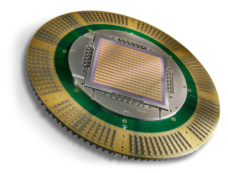
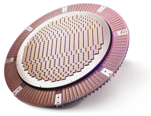
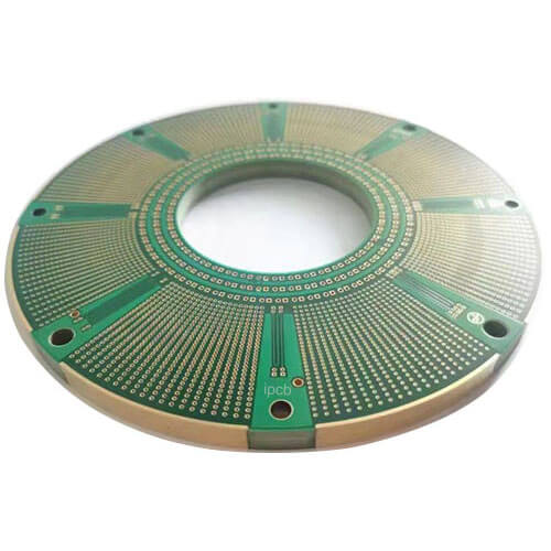
Structure of a Probe Card PCB
A typical Probe Card PCB includes:
- High-density interconnect layers
- Precision pads for probe alignment
- Controlled impedance traces
- Interface connectors for ATE systems
The Probe Card PCB acts as a signal distribution platform, connecting hundreds or thousands of test channels.
Key Requirements of Probe Card PCB
1. Ultra-High Precision
Probe Card PCB fabrication requires extremely tight tolerances for alignment and pad positioning.
2. Controlled Impedance
Essential for high-speed and RF semiconductor testing.
3. High Layer Count & Density
Probe Card PCB designs often require multilayer structures with complex routing.
4. Excellent Planarity
Flatness is critical to ensure consistent probe contact with wafer pads.
5. Thermal Stability
The Probe Card PCB must maintain performance under varying test temperatures.
Types of Probe Card PCB Applications
1. Cantilever Probe Cards
Use needle-like probes mounted on the Probe Card PCB.
2. Vertical Probe Cards
High-density probe arrays for advanced ICs.
3. MEMS Probe Cards
Microfabricated probes integrated with high-density Probe Card PCB designs.
Materials for Probe Card PCB
Material selection depends on frequency, density, and thermal requirements:
- High Tg FR4 → standard applications
- BT Epoxy → IC substrate-level stability
- Low loss materials → high-speed testing
- Ceramic materials → high thermal stability
Signal Integrity in Probe Card PCB
Signal Integrity∝1Loss+Impedance Mismatch\text{Signal Integrity} \propto \frac{1}{\text{Loss} + \text{Impedance Mismatch}}Signal Integrity∝Loss+Impedance Mismatch1
https://www.kkpcba.com/ate-pcb-probe-card/Probe Card PCB must minimize:
- Signal loss
- Crosstalk
- Reflection
Manufacturing Challenges of Probe Card PCB
Producing a high-quality Probe Card PCB involves:
1. Tight Tolerance Fabrication
Micron-level accuracy is required for pad alignment.
2. Multilayer Registration
Precise alignment across layers is critical.
3. Surface Finish Control
Ensures reliable probe contact and durability.
4. Yield Management
High density increases defect risk.
Applications of Probe Card PCB
1. Wafer-Level Testing
Ensures chip functionality before packaging.
2. High-Speed IC Testing
Supports high-frequency signal validation.
3. Automotive Semiconductor Testing
High reliability requirements.
4. Advanced Packaging (BGA, CSP)
Verification before final assembly.
When Do You Need a Probe Card PCB?
You need a Probe Card PCB when:
- Performing wafer-level IC testing
- Developing semiconductor test systems
- Requiring high-precision electrical measurement
- Integrating with ATE systems
