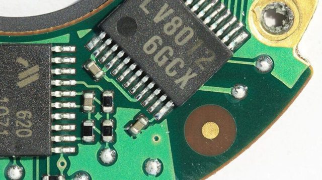
As electronic systems become more powerful and complex, standard multilayer PCBs are sometimes no longer sufficient. Advanced applications such as telecommunications infrastructure, data servers, and aerospace electronics often require extremely dense routing and precise signal control.
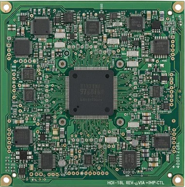
This is where High Layer Count PCBs come into play. These circuit boards typically contain 20 layers or more, allowing engineers to manage large numbers of signals, power networks, and ground planes within a compact design.
High layer count PCBs provide the electrical architecture needed to support modern high-performance electronics.
What Is a High Layer Count PCB?

A High Layer Count PCB refers to a multilayer printed circuit board with a significantly large number of copper layers, commonly starting from 20 layers and extending to 40 layers or more.
Each layer serves a specific function, such as:
• signal routing layers
• power distribution planes
• ground reference planes
• shielding layers for noise reduction
By stacking multiple layers together, engineers can route thousands of connections while maintaining stable electrical performance.
Key Advantages of High Layer Count PCBs
Higher Circuit Density
More layers allow designers to route complex circuits without increasing the board size.
Improved Signal Integrity
Dedicated ground and power planes help reduce electromagnetic interference and signal noise.
Better Power Distribution
Multiple power planes ensure stable voltage delivery across complex systems.
Compact System Design
High layer count boards enable powerful electronic systems to fit into smaller devices.
Design Challenges of High Layer Count PCBs

While these boards offer significant benefits, they also introduce substantial engineering challenges.
Complex Stack-Up Design
Proper layer arrangement is essential to maintain impedance control and minimize signal interference.
Thermal Management
Dense circuitry can generate heat that must be carefully managed through copper distribution and materials.
Manufacturing Precision
Layer alignment tolerance becomes extremely critical when stacking dozens of layers together.
Signal Integrity for High-Speed Interfaces
Interfaces such as PCIe, DDR memory, and high-speed networking require precise impedance control.
Materials Used in High Layer Count PCBs
Material selection plays a major role in the performance of high-layer boards.
Common materials include:
High-Tg FR-4 laminates
Provide mechanical stability for complex multilayer structures.
Low-loss dielectric materials
Used in high-speed digital and RF applications to reduce signal attenuation.
High-performance laminates
Required for advanced telecom or aerospace electronics.
Material stability is essential because even slight expansion differences can affect layer alignment.
Typical Applications
High layer count PCBs are widely used in industries where circuit complexity and signal speed are extremely high.
Telecommunications Equipment
5G base stations and networking infrastructure require complex multilayer routing.
Data Center Servers
High-performance processors and memory subsystems demand advanced PCB architectures.
Aerospace and Defense
Mission-critical electronics often use high-layer boards for reliability and signal control.
Medical Imaging Equipment
Systems such as MRI and CT scanners rely on high-density circuit boards.
Why High Layer Count PCBs Are Critical for Modern Electronics
The demand for faster processing, higher bandwidth, and smaller devices continues to push PCB technology forward. High layer count PCBs enable engineers to design extremely complex systems while maintaining electrical stability and reliability.
From high-speed servers to advanced telecommunications hardware, these multilayer structures form the backbone of modern electronic innovation.
As computing power and data throughput continue to grow, High Layer Count PCB technology will remain essential in supporting the next generation of electronics.
