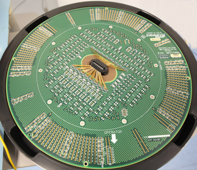
Probe Card PCB Assembly is a highly specialized PCB assembly process designed for semiconductor wafer testing applications. Probe cards act as the critical interface between automated test equipment (ATE) and semiconductor wafers, making assembly accuracy and reliability essential for precise electrical measurement.
As semiconductor devices move toward smaller nodes, higher pin counts, and faster test speeds, professional probe card PCB assembly services are required to meet increasingly demanding performance and reliability standards.
What Is Probe Card PCB Assembly?
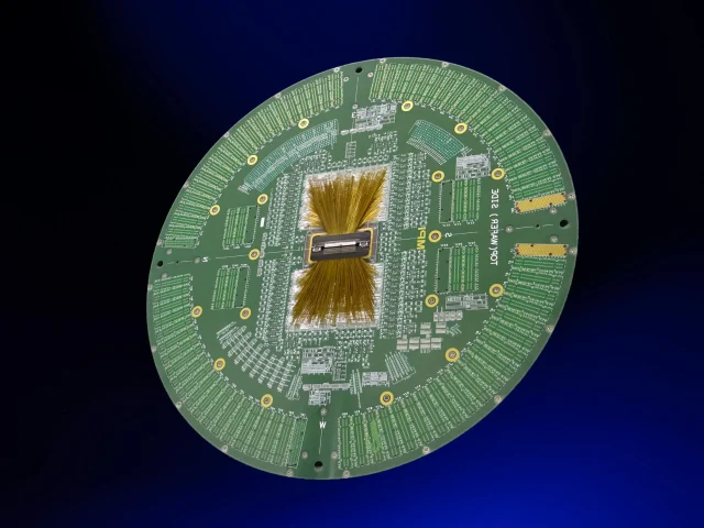
Probe Card PCB Assembly refers to the assembly of printed circuit boards used in semiconductor probe cards. These PCBs support probe needles, MEMS probes, connectors, and interface circuits that deliver test signals from ATE systems to individual die on a wafer.
Unlike conventional PCB assembly, probe card PCB assembly must achieve extremely tight tolerances, stable mechanical structures, and consistent electrical performance across thousands or millions of test cycles.
Key Requirements for Probe Card PCB Assembly
Ultra-High Precision Assembly
Probe card PCBs require precise alignment of probes, connectors, and components to ensure accurate contact with wafer pads.
High Pin Count and Dense Interconnects
Modern probe cards support thousands of signal channels, requiring advanced assembly techniques for high pin count connectors and dense routing.
Signal Integrity and Controlled Impedance
High-speed digital and RF wafer testing demands strict impedance control and low signal loss throughout the assembled PCB.
Mechanical Stability and Durability
Probe card assemblies must withstand repeated probe contact, thermal cycling, and mechanical stress during wafer testing.
Assembly Capabilities for Probe Card PCB Assembly
 Advanced services tpically include:
-
High-precision SMT and mixed assembly
-
Fine-pitch, micro-pitch, and high pin count component assembly
-
BGA, LGA, QFN, and custom connector assembly
-
Controlled soldering profiles for dimensional stability
-
Precision socket and interface connector installation
-
AOI, X-ray inspection, and functional testing
These capabilities ensure stable electrical and mechanical performance throughout the probe card lifecycle.
Materials and PCB Structures for Probe Card Assembly
Probe card PCB assembly often utilizes specialized PCB designs and materials, including:
-
Multilayer and high layer count PCBs
-
Controlled impedance and high-speed PCB structures
-
Low-loss materials for RF and high-frequency testing
-
Thick copper and reinforced PCB constructions
-
Hybrid rigid, rigid-flex, or HDI PCB designs
Material selection plays a critical role in test accuracy and long-term reliability.
Quality Control and Engineering Support
Due to the critical role of probe cards in semiconductor testing, quality control is a core element of probe card PCB assembly:
-
DFM and DFA analysis prior to assembly
-
Precision process control and traceability
-
In-process inspection and post-assembly verification
-
Electrical continuity and functional testing
-
Assembly documentation and quality reporting
Close collaboration between engineering and assembly teams helps minimize probe alignment issues and signal integrity risks.
Applications of Probe Card PCB Assembly
Probe card PCB assembly is widely used in:
-
Wafer sort and wafer-level testing
-
Logic and memory semiconductor testing
-
RF and mmWave device testing
-
Automotive and high-reliability IC testing
-
Advanced node semiconductor production
In these applications, assembly precision directly impacts test yield and throughput.
Prototype and Volume Probe Card PCB Assembly
Probe card PCB assembly projects typically start with prototype or pilot builds to validate mechanical alignment, electrical performance, and assembly processes. Once confirmed, the same high-precision processes are scaled to volume production with strict consistency control.
Working with a single supplier capable of both PCB fabrication and probe card PCB assembly simplifies communication, reduces risk, and improves overall delivery efficiency.
Conclusion
Probe Card PCB Assembly is a mission-critical process in semiconductor wafer testing. Through high-precision assembly techniques, advanced inspection methods, and rigorous quality control, professional probe card PCB assembly providers ensure reliable test performance across high-volume semiconductor production.
As semiconductor testing requirements continue to evolve, selecting an experienced probe card PCB assembly partner is essential for achieving accuracy, reliability, and long-term test stability.
