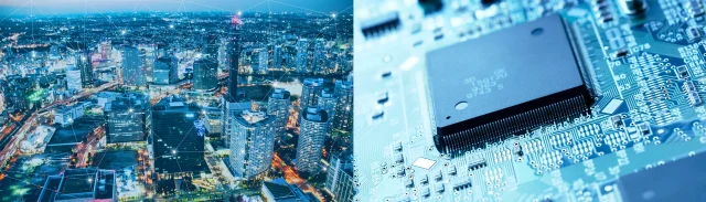
A BT Epoxy PCB is a specialized organic substrate widely used in IC packaging, semiconductor interposers, and high-density electronic modules. BT (Bismaleimide Triazine) epoxy resin materials are engineered to provide enhanced thermal stability, low moisture absorption, and excellent dimensional control, making BT Epoxy PCBs a preferred choice for fine-pitch and high-I/O-count packaging environments.
Unlike standard FR-4 materials, BT epoxy substrates are optimized for applications where package-level reliability and electrical consistency are critical to overall device performance.
Material Characteristics of BT Epoxy PCBs
The core advantage of a BT Epoxy PCB lies in the molecular structure of BT resin, which offers improved thermal and mechanical performance compared to conventional epoxy systems.
Key material properties of BT Epoxy PCBs include:
-
Higher glass transition temperature (Tg) than standard FR-4
-
Low coefficient of thermal expansion (CTE) for dimensional stability
-
Low moisture absorption to reduce package delamination risk
-
Stable dielectric properties for fine-pitch signal routing
These properties make BT Epoxy PCBs well suited for IC substrates and high-density packaging structures.
Electrical Performance and Signal Integrity
In IC packaging and substrate-level routing, maintaining electrical consistency across dense interconnects is essential. BT Epoxy PCB materials provide predictable dielectric behavior that supports controlled impedance routing in compact layouts.
Electrical benefits include:
-
Stable dielectric constant across temperature ranges
-
Reduced signal skew in high-density routing environments
-
Improved impedance consistency for high-speed interfaces
-
Reliable performance in multi-layer substrate designs
These characteristics are critical for memory packages, processors, and high-speed logic devices.
Thermal Stability and Package Reliability
Thermal cycling is a major stress factor in semiconductor packaging. BT Epoxy PCBs are engineered to maintain structural integrity under repeated temperature excursions.
Thermal and reliability advantages include:
-
Reduced warpage during reflow and assembly
-
Improved solder joint reliability
-
Enhanced resistance to thermal fatigue
-
Stable performance under long-term operating temperatures
By minimizing mechanical stress, BT Epoxy PCBs help extend package lifespan and yield.
Manufacturing and Process Considerations
BT Epoxy PCB fabrication requires tighter process control than standard PCB manufacturing due to fine line widths and tight dimensional tolerances.
Critical manufacturing considerations include:
-
Precise lamination control for multilayer stackups
-
Fine-line etching capability for dense routing
-
Controlled drilling and via formation
-
Strict moisture control throughout fabrication
Manufacturing consistency is essential to ensure electrical and mechanical reliability across production lots.
Typical Applications of BT Epoxy PCBs
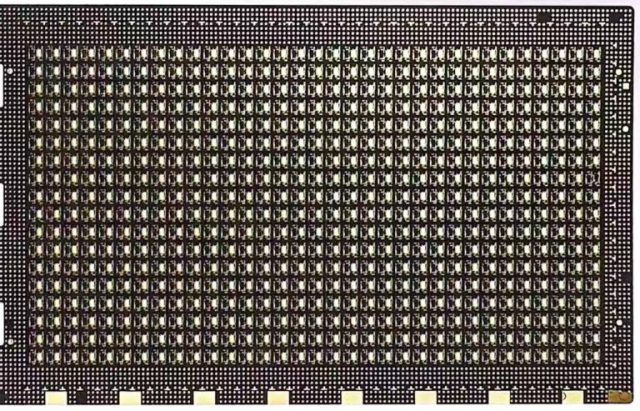
BT Epoxy PCBs are commonly used in:
-
IC substrates and semiconductor packages
-
Ball Grid Array (BGA) and Chip Scale Package (CSP) substrates
-
High-density interposer boards
-
Memory modules and processor packaging
-
Advanced consumer and industrial electronics
In these applications, BT Epoxy PCBs bridge the gap between silicon devices and system-level PCBs.
Engineering Perspective
A BT Epoxy PCB is not a general-purpose circuit board—it is a material-driven packaging solution designed to support high-density interconnects, thermal stability, and long-term reliability. Proper selection and processing of BT epoxy materials enable consistent electrical performance and robust mechanical behavior in advanced electronic packaging.
KKPCB supports BT Epoxy PCB manufacturing through disciplined material selection, fine-line fabrication capability, and strict process control tailored to IC packaging requirements.
