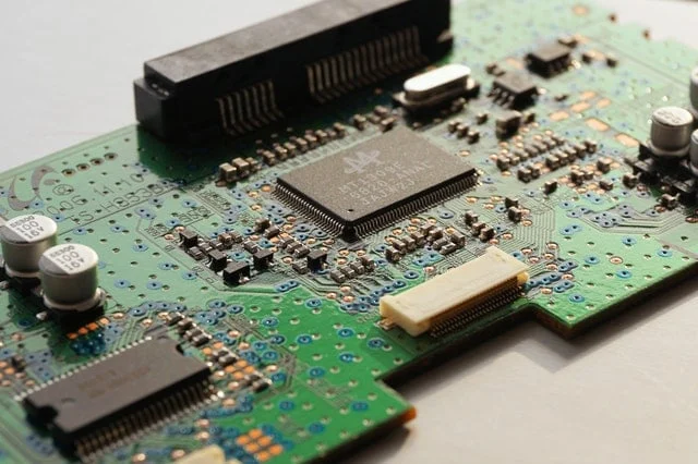
As semiconductor devices continue to scale in speed, density, and complexity, IC testing PCB has become a critical component in ensuring chip performance, reliability, and yield. From wafer-level testing to final package validation, IC testing PCBs act as the electrical interface between the device under test (DUT) and automated test equipment (ATE).
High-quality IC testing PCBs are essential for accurate signal transmission, stable power delivery, and repeatable test results throughout the semiconductor development and production lifecycle.
What Is an IC Testing PCB?
An IC Testing PCB is a specialized printed circuit board designed specifically for semiconductor testing environments. It is commonly used in:
-
IC functional testing
-
Parametric testing
-
Burn-in and reliability testing
-
Final test and system-level validation
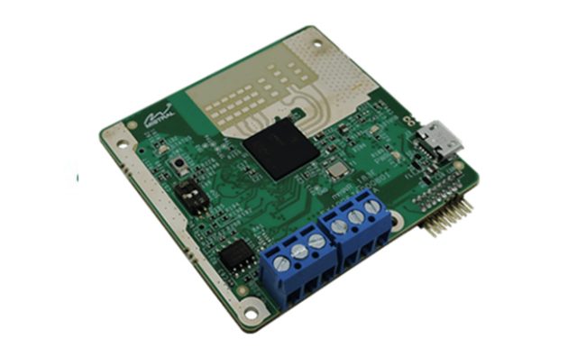
IC testing PCBs are often integrated into load boards, probe cards, test sockets, and ATE interfaces, requiring extremely high electrical and mechanical precision.
Key Design Challenges of IC Testing PCB
Unlike standard PCBs, IC testing PCBs must meet strict electrical and structural requirements to ensure test accuracy and repeatability.
High-Speed Signal Integrity
Modern IC testing PCBs support high-speed digital and RF signals, requiring:
-
Controlled impedance traces
-
Low-loss materials
-
Tight length matching and skew control
Signal integrity issues directly affect test accuracy, making PCB design quality critical.
High Pin Count and Fine Pitch
Advanced ICs often feature:
-
High pin counts
-
Fine-pitch pads and connectors
-
Dense BGA or socket interfaces
IC testing PCBs must support HDI structures, microvias, and multilayer stackups to accommodate complex routing.
Power Integrity and Thermal Stability
Stable power delivery is essential during IC testing, especially for high-performance chips. IC testing PCBs are designed with:
-
Low-impedance power planes
-
Decoupling optimization
-
Thermal control for long test cycles
Materials and Stackups for IC Testing PCB
Material selection plays a crucial role in IC testing PCB performance. Depending on test frequency and environment, common materials include:
-
High-Tg FR-4 for standard IC testing
-
Low-loss laminates for high-speed and RF ICs
-
Hybrid stackups combining FR-4 and high-frequency materials
-
Specialized materials for high-temperature or burn-in testing
Stackup design is closely tied to impedance control and mechanical stability.
IC Testing PCB Manufacturing Capabilities
Manufacturing IC testing PCBs requires advanced process control and strict tolerances.
Typical IC testing PCB features include:
-
Multilayer construction (8–40+ layers)
-
HDI structures with microvias and buried vias
-
Controlled impedance fabrication
-
Tight thickness and flatness control
High-quality fabrication ensures repeatable electrical performance across multiple test cycles.
Small Batch and Prototype IC Testing PCB
IC testing PCBs are frequently produced in small batches or prototype volumes, especially during new IC development or test program validation.
Small-batch IC testing PCB advantages:
-
Fast delivery for engineering validation
-
Flexible design iterations
-
Early detection of signal or layout issues
-
Smooth transition to volume testing
Rapid prototyping shortens test development cycles and reduces overall project risk.
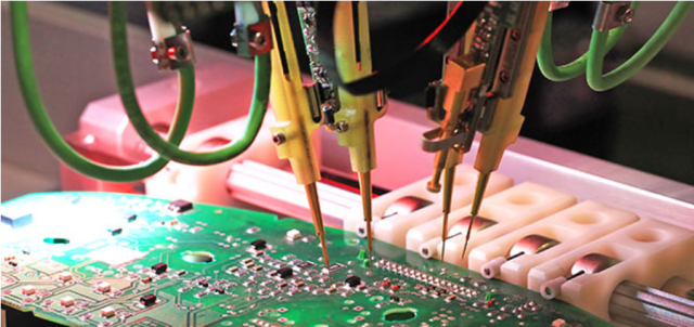
IC Testing PCB Assembly and Quality Control
In addition to fabrication, IC testing PCB assembly demands high precision. Common assembly features include:
-
Fine-pitch SMT assembly
-
High-pin-count connectors and sockets
-
Press-fit or hybrid assembly processes
Quality control for IC testing PCB typically includes:
-
AOI and X-ray inspection
-
Electrical continuity testing
-
Impedance verification
These steps ensure consistent performance in demanding test environments.
Why Choose KKPCB for IC Testing PCB
KKPCB specializes in IC testing PCB manufacturing for semiconductor and ATE applications. With strong capabilities in HDI, multilayer, high-speed, and controlled impedance PCB fabrication, KKPCB supports customers from early test development to stable production.
Whether for load boards, probe card PCBs, or custom IC test interfaces, KKPCB delivers reliable, engineering-driven solutions with fast turnaround and consistent quality.
