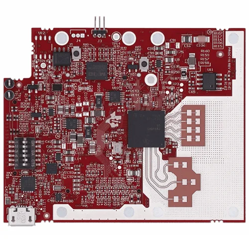
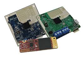
High-frequency mmWave module PCB architectures define the performance boundary of 28–60 GHz wireless platforms, where beamforming accuracy, ultra-low-loss routing, and tight impedance control determine every detail of system efficiency. In dense phased-array units, even microscopic changes in Dk/Df, copper roughness, dielectric uniformity, or via transition geometry produce measurable degradation in beam steering vectors, noise floors, EVM, and array coherence.
Next-generation mmWave PCB engineering demands multilayer structures tuned for low insertion loss, wideband phase linearity, and high-isolation RF propagation across each antenna chain.
High-Frequency Constraints in 28–60 GHz mmWave PCB Systems
In mmWave domains, PCB performance is dictated by electromagnetic behavior at sub-millimeter scales:
The RF chain must satisfy:
• Ultra-low-loss transmission across microstrip/GCPW lines
• ±0.5° beamforming phase accuracy across multi-antenna arrays
• Stable Dk/Df to prevent beam squint, group delay drift, and mode imbalance
• High isolation between tightly spaced RF paths
• Thermally stable dielectric properties under PA/LNA heat loads
• High-Q routing minimizing distortion and intermodulation products
These constraints force PCB engineers to adopt low-Df PTFE/hydrocarbon laminates, hybrid multi-dielectric stackups, and advanced high-frequency interconnect techniques.
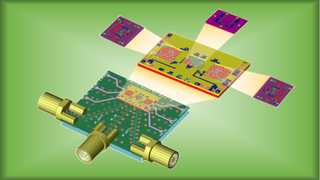
Low-Loss mmWave PCB Stackups Built for Wideband RF Transmission
To maintain consistent amplitude and phase distribution across phased-array modules, mmWave PCB stackups must deliver repeatable RF behavior across temperature, frequency, and manufacturing variance.
V5.0 stackup principles include:
• Dielectrics with Df ≤ 0.002 to suppress wideband RF dissipation
• Dk uniformity ±0.02 enabling tightly matched electrical lengths
• Hybrid PTFE + Megtron + PPO structures balancing low loss and rigidity
• Smooth rolled copper (Ra < 0.7 µm) for reduced conductor loss through 28–60 GHz
• Uniform bonding films eliminating height-induced phase discontinuity
These constructions preserve RF phase coherence, reduce insertion loss, and stabilize the propagation constant across every beamforming channel.
Impedance-Controlled Routing for Ultra-Clean mmWave Channel Integrity
At mmWave, impedance error becomes a dominant source of reflection and phase distortion.
V5.0 routing strategies emphasize:
• GCPW structures engineered for ±2% impedance tolerance
• Stripline/microstrip transitions tuned through HFSS/ADS optimization
• Back-drilled via stubs to eliminate unwanted resonances at 30–60 GHz
• HDI blind/buried vias minimizing vertical parasitics
• RF shielding, segmented grounds, and isolation corridors to suppress crosstalk
• Anti-pad shaping + reference plane stitching for mode-conversion suppression
These methods keep S-parameters exceptionally stable, enabling high-Q propagation and linear beam steering.
Thermal and Mechanical Stability for High-Power Beamforming Arrays
mmWave beamforming ICs and PAs generate concentrated thermal loads.
Thermal disturbances alter line impedance, stackup height, and dielectric constants.
V5.0 architectures incorporate:
• Thermal vias, via farms, and copper coins for vertical heat extraction
• Low-CTE laminates maintaining layer registration under thermal cycling
• Graphite and copper hybrid planes distributing temperature uniformly
• High-Tg resins sustaining stability during 5G high-power duty cycles
This ensures stable signal propagation and predictable phase responses during full-band operation.
System-Level Impact on 28–60 GHz Wireless Platforms
Engineered mmWave module PCB architectures directly improve:
• Beamforming resolution & vector precision
• Low-loss transmission line performance
• Wideband phase linearity across dynamic RF loads
• Array coherence in 5G massive-MIMO and SATCOM terminals
• Thermal reliability under continuous high-power operation
• EMI/EMC robustness in tightly integrated RF front-ends
These enhancements elevate the entire system, enabling high-capacity wireless communication, accurate sensing, and stable wideband RF links.
Summary
Next-generation mmWave module PCB architectures must simultaneously deliver ultra-stable dielectric performance, low-loss routing, high-isolation RF propagation, and phase-accurate beamforming across every 28–60 GHz channel.
Through engineered multilayer stackups, hybrid dielectric systems, precision impedance-controlled routing, and thermally optimized interconnects, mmWave platforms achieve the RF purity and wideband stability demanded by modern wireless systems.
