RO4350B PCB materials are widely deployed in 5G smartphone RF front-end modules because they provide a balanced dielectric profile, low-loss characteristics, and stable RF transmission up to sub-6 GHz and selected mmWave bands. Modern antenna arrays, PA/LPF modules, LNA chains, and tunable impedance networks face stringent constraints in signal integrity, power density, EMI coupling, and thermal rise due to the compact form factor of handheld devices. This article focuses on building a practical engineering framework that shows how RO4350B supports high-efficiency RF chains, predictable impedance control, and thermally balanced integration across multi-band 5G smartphone platforms.
Core Engineering Challenges
5G smartphones compress an increasingly complex RF chain into a few square centimeters. This creates several engineering bottlenecks:
Signal Integrity Constraints
High-Q transmission lines used for 3–7 GHz bands are sensitive to insertion loss, surface roughness, and microstrip width mismatch. RO4350B’s dielectric tolerance helps mitigate these effects, but routing density and antenna proximity still impact RF linearity.
Power Density & Thermal Effects
PA efficiency peaks generate localized heat zones. If the laminate exhibits high CTE mismatch or thermal resistance, the RF chain experiences gain drift, IMD (intermodulation distortion), and degraded ACLR (adjacent channel leakage ratio).
EMI Coupling Between Bands
Smartphones integrate multiple antennas and harmonic filters in close quarters. Without controlled dielectric behavior and precise stackup transitions, near-field coupling increases, reducing isolation.
Mechanical & Miniaturization Stress
Thinner stackups (<0.8 mm) can induce bending stress during assembly. The laminate must sustain solder reflow, multi-temperature cycles, and mechanical shock without delamination or impedance drift.
Material Science & Dielectric Performance
RO4350B provides a controlled Dk of 3.48 ±0.05, low dissipation factor, and stable dielectric properties across wide temperature ranges. The predictable dielectric response is particularly useful for short-wavelength RF routing.
Material Parameter Table
| Parameter | Typical Value | Impact on RF Design |
|---|---|---|
| Dielectric Constant (10 GHz) | 3.48 | Predictable impedance & phase velocity |
| Dissipation Factor | 0.0037 | Reduced insertion loss |
| Thermal Conductivity | 0.64 W/m·K | Improved heat spreading vs FR-4 |
| CTE (Z-axis) | 46 ppm/°C | Stable multilayer bonding |
| Glass Transition Temperature | >280°C | Supports reflow cycles |
The dielectric stability of RO4350B ensures that antenna feed accuracy, PA output filtering, and matching networks maintain repeatability across batches and temperature sweeps.
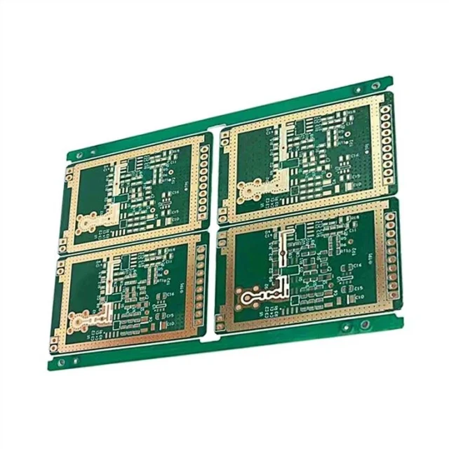
KKPCB Case Study —5G Smartphone RF Front-End PCB
Engineering Scenario
A smartphone manufacturer required an RF front-end board for a dual-sub-6G 5G platform. The design included PA, LNA, tunable matching networks, and antenna feedlines in a compact boundary.
Customer Requirements
• Reduce insertion loss on 3.5 GHz and 4.9 GHz channels
• Improve PA thermal spreading to avoid output power drift
• Enhance EMI isolation between duplex bands
• Maintain consistent impedance across batch production
Engineering Challenges
• Routing density limited microstrip width options
• Proximity to metal shielding introduced parasitic capacitance
• High-power PA area risked local hotspots
• Isolation between RX/TX lines required careful ground stitching
KKPCB Engineering Solution
• Hybrid RO4350B + FR-4 stackup for localized RF performance
• Modified microstrip geometry to reduce conductor loss
• Copper roughness optimized using low-profile foil in RF zones
• Thermal vias placed beneath PA module for better heat evacuation
• Isolation walls and staggered stitching vias implemented
Measurement Result Table
Test Item |
Before Optimization |
After Optimization |
|---|---|---|
| Insertion Loss @ 3.5 GHz | 0.72 dB | 0.42 dB |
| PA Temperature Rise | 38°C | 24°C |
| RX/TX Isolation | 21 dB | 30 dB |
| Impedance Deviation | ±12% | ±4% |
| Harmonic Rejection | 13 dB | 19 dB |
The combined effect was a measurable gain improvement and higher RF repeatability across 20 production lots.
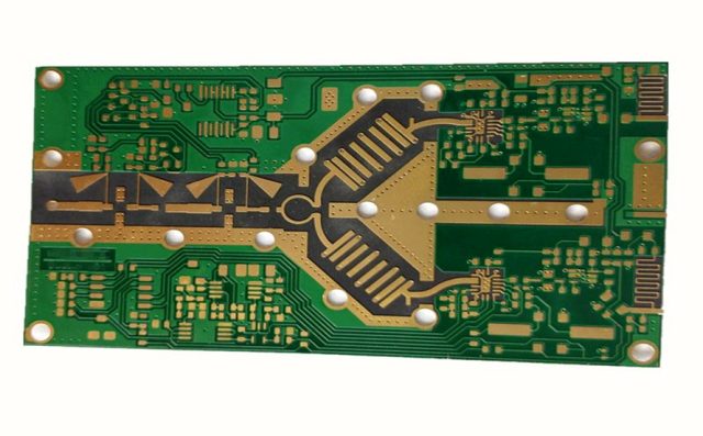
Stackup Design & RF Implementation
The hybrid stackup leverages RO4350B’s RF advantages while reducing cost through localized deployment.
Example Stackup Table
Layer |
Material |
Thickness |
Function |
|---|---|---|---|
| L1 | RO4350B | 0.1 mm | RF routing, antenna feed |
| L2 | Copper | — | RF ground |
| L3 | FR-4 | 0.2 mm | Control circuits |
| L4 | FR-4 | 0.2 mm | Base ground |
Key RF Implementation Notes
• Antenna feedlines simulated in HFSS using 4-mil width to maintain 50Ω impedance
• ADS used to tune matching network including series-shunt topology
• TDR measurements confirmed impedance consistency
• Ground via fences designed with ≤1 mm spacing to suppress EMI
• Thermal FEM verified PA region delta-T under max transmit power
Environmental & Reliability Validation
Reliability Test Table
Test Item |
Condition |
Result |
|---|---|---|
| Thermal Cycling | −40°C to 125°C, 500 cycles | No delamination, impedance drift <2% |
| Humidity Stress | 85°C / 85% RH, 500 hrs | Loss increase <0.05 dB |
| Mechanical Drop | 1 m drop, 10 cycles | No cracking |
| Reflow Simulation | 260°C × 3 cycles | No blistering |
| Vibration Test | 10–200 Hz sweep | Stable RF response |
These results demonstrate the ability of RO4350B to maintain long-term RF reliability in thin smartphone stackups.
Engineering Summary & Contact
RO4350B PCB materials provide a practical balance between RF performance, manufacturability, thermal stability, and cost for 5G smartphone RF front-end systems. Their stable dielectric profile supports low-loss routing, predictable impedance, and improved PA thermal behavior, enabling consistent multi-band antenna performance. When paired with careful microstrip optimization, thermal via design, EMI shielding, and hybrid stackups, RO4350B becomes a highly reliable solution for modern handheld RF architectures.
